-

This Power MOSFET provides the circuit designer with the best combination of fast switching, ruggedized device design, low on-resistance and cost-effectiveness.
-
-19%
 Out Of Stock
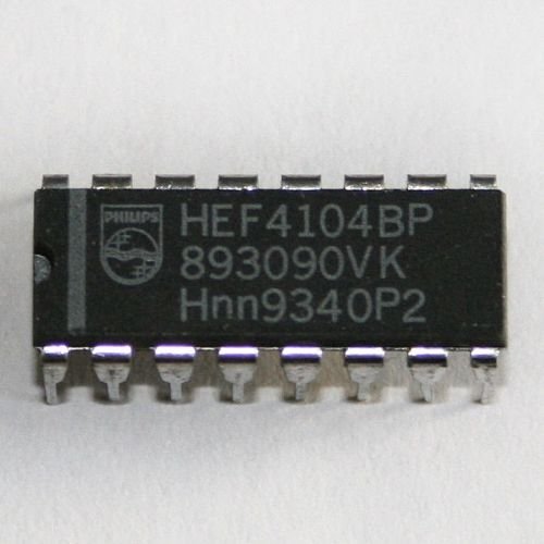
The AD7528 is a monolithic dual 8-bit digital/analog converter featuring excellent DAC-to-DAC matching. It is available in skinny 0.3″ wide 20-lead DIPs and in 20-lead surface mount packages. Separate on-chip latches are provided for each DAC to allow easy microprocessor interface.
-
-21%
SCR C106 C106 Series – SCR TO-255AA 4A
Original price was: ₨75.00.₨59.00Current price is: ₨59.00. Quick View- Glassivated Surface for Reliability and Uniformity
- Power Rated at Economical Prices
- Practical Level Triggering and Holding Characteristics
- Flat, Rugged, Thermopad Construction for Low Thermal Resistance, High Heat Dissipation and Durability
- Sensitive Gate Triggering
- Device Marking: Device Type, e.g., C106B, Date Cod
-
-16%
- Logic Type: INVERTER / NOR / NAND
- Output Current: 6.8mA
- Supply voltage range: 3V to 18V
- Package Type: DIP
- Pin number: 14
- Operating temperature range: -55 ° C to +125 ° C
- Surface Mount Devices: through-hole mounting
-

- Low saturation voltage
- Simple drive requirements
- High safe operating area
- For low distortion complementary designs
- Easy to carry and handle
-

- N-Channel Power MOSFET
- Continuous Drain Current (ID): 10A
- Gate threshold voltage (VGS-th) is 10V (limit = 20V)
- Drain to Source Breakdown Voltage: 400V
- Drain Source Resistance (RDS) is 0.55 Ohms
- Rise time and fall time is 27nS and 24nS
- Available in To-220 package
-
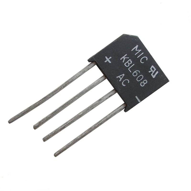
Bridge rectifier diode with a 6A current rating.
-

The TL494 device incorporates all the functions required in the construction of a pulse-width-modulation (PWM) control circuit on a single chip. Designed primarily for power-supply control, this device offers the flexibility to tailor the power-supply control circuitry to a specific application. The TL494 device contains two error amplifiers, an on-chip adjustable oscillator, a dead-time control (DTC) comparator, a pulse-steering control flip-flop, a 5-V, 5%-precision regulator, and output-control circuits.The TL494C device is characterized for operation from 0C to 70C. The TL494I device is characterized for operation from 40C to 85C.
-
-8%

This Tri-state bi-directional transceiver utilize advanced silicon-gate CMOS technology and is intended for two-way asynchronous communication between data buses. They have high drive current outputs which enable high speed operation even when driving large bus capacitances. The circuit possess the low power consumption of CMOS circuitry, yet have speeds comparable to low power Schottky TTL circuits.
-
-28%
74LS47 IC – Common Anode LED Driver
Original price was: ₨90.00.₨65.00Current price is: ₨65.00. Quick View74LS47 is a BCD to 7-segment decoder/driver IC. It accepts a binary coded decimal as input and converts it into a pattern to drive a seven-segment for displaying digits 0 to 9.
-
-54%
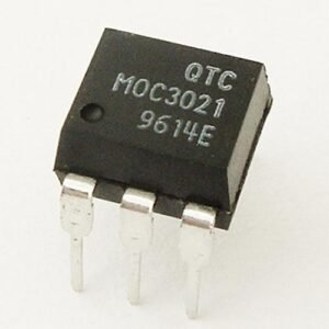
MOC3021 Triac Driven Optoisolator
Original price was: ₨150.00.₨69.00Current price is: ₨69.00. Quick View- Opto-isolator with Zero-Crossing Triac Driver
- Input LED Diode Forward Voltage: 1.15V
- LED Forward Latch Current: 15mA
- TRIAC output terminal voltage: 400V (max)
- TRIAC peak output current: 1A
- Available as 6-pin PDIP with and without M-suffix
-
-19%

This laser pointer or laser pen is a small handheld device with a laser diode emitting a very narrow coherent low-powered laser beam of visible light, it is frequently used in lecture halls and demonstrations to point at topics of interest on a presentation board. In a school setting, they have become ubiquitous, and they are very useful teaching aids.
-
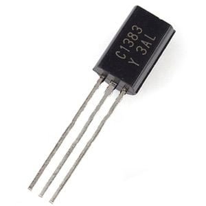
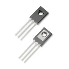
C1383 is a Bipolar NPN type transistor which is used for low-frequency power amplification and driver amplification.
-
-14%

- Type: NPN
- Collector-Emitter Voltage, max: 140 V
- Collector-Base Voltage, max: 140 V
- Emitter-Base Voltage, max: 5 V
- Collector Current − Continuous, max: 10 A
- Collector Dissipation: 100 W
- DC Current Gain (hfe): 55 to 160
- Transition Frequency, min: 30 MHz
- Operating and Storage Junction Temperature Range: -55 to +150 °C
- Package: TO-3P
-
-14%

- Type –NPN
- Collector-Emitter Voltage: 400V
- Collector-Base Voltage: 450V
- Emitter-Base Voltage: 7V
- Collector Current: 10A
- Collector Dissipation – 80W
- DC Current Gain (hfe) – 10
- Operating and Storage Junction Temperature Range -55 to +150C
-

- High-Voltage Types (20V Rating)
- CD4071BMS Quad 2-Input OR Gate
- CD4072BMS Dual 4-Input OR Gate
- CD4075BMS Triple 3-Input OR Gate
- Medium Speed Operation: tPHL, tPLH = 60ns (typ) at 10V
- 100% Tested for Quiescent Current at 20V
- Maximum Input Current of 1A at 18V Over Full Package Temperature Range; 100nA at 18V and +25oC
- Standardized Symmetrical Output Characteristics
-
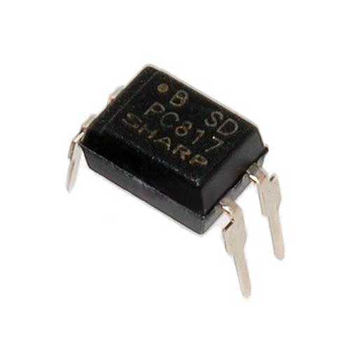
Optocoupler 817 QUAD contains an IRED optically coupled to a phototransistor. It is packaged in a 4pin DIP, available in wide-lead spacing option and SMT gullwing lead-form option. Input-output isolation voltage(rms) is 5.0kV. Collector-emitter voltage is 80V(*) and CTR is 50% to 600% at input current of 5mA.
-
-22%
 Out Of Stock
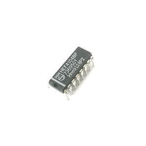
The HEF4104B is a quad low voltage-to-high voltage translator with 3-state outputs. It provides the capability of interfacing low voltage circuits to high voltage circuits. For example low voltage Local Oxidation Complementary MOS (LOCMOS) and Transistor-Transistor Logic (TTL) to high voltage LOCMOS. It has four data inputs (A0 to A3), an active HIGH output enable input (OE), four data outputs (B0 to B3) and their complements (B0 to B3).
-
-30%
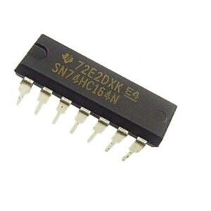
74HC164 8-Bit Parallel-Out Shift Register
Original price was: ₨100.00.₨70.00Current price is: ₨70.00. Quick ViewFeatures/Specs:
Wide Supply Voltage Range from 2.0V to 6.0V
Sinks or Sources 4mA at VCC = 4.5V
CMOS Low Power Consumption
Schmitt Trigger Action at all Inputs
ESD Protection Exceeds JESD 22v 200-V Machine Model (A115)
2000-V Human Body Model (A114)
Exceeds 1000-V Charged Device Model (C101)
Range of Package Options SO-14 and TSSOP-14
Totally Lead-Free & Fully RoHS Compliant
Halogen and Antimony Free. Green Device
-
- Op-amp coupled with MOSFET at output
- Wide power supply Range
- Singe supply – 5V to 16V
- Dual supply – ±2.5V to ±8V
- Input Terminal current: 1mA
- Maximum Output Voltage: 13.3V
- Maximum source current: 22mA
- Maximum sink current: 20mA
- Supply current: 10mA
- Common Mode Rejection Ration (CMRR): 80dB
-

It is an integrated circuit that converts the signals from the RS232 serial port to the proper signal which is used in the TTL compatible digital logic circuits. The MAX232 can convert the signals like RX, TX, CTS, and RTS and it is a dual driver/receiver.
-
-20%
The uA723 is a precision integrated-circuit voltage regulator, featuring high ripple rejection, excellent input and load regulation, excellent temperature stability, and low standby current. The circuit consists of a temperature-compensated reference-voltage amplifier, an error amplifier, a 150-mA output transistor, and an adjustable-output current limiter.The uA723 is characterized for operation from 0C to 70C.
-
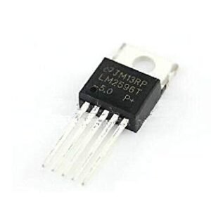
- 3.3V, 5V, 12V, and adjustable output versions
- Adjustable version output voltage range, 1.2V to 37V ±4% max over line and load conditions
- Available in TO-220 and TO-263 packages
- Guaranteed 3A output load current
- Input voltage range up to 40V
- Requires only 4 external components
- Excellent line and load regulation specifications
- 150 kHz fixed frequency internal oscillator
- TTL shutdown capability
- Low power standby mode, IQ typically 80 µA
- High efficiency
- Uses readily available standard inductors
- Thermal shutdown and current limit protection
-
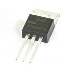
- Maximum Terminal current: 4A
- On-state Gate voltage: 1.4V
- Gate trigger current: 10mA
- Max Terminal Voltage is 600 V
- Holding current: 2.2mA
- Latching current: 4mA
- Available in To-220 Package
-
-20%
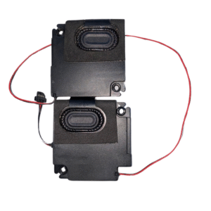
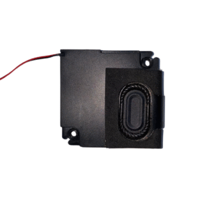
- Resistance: 8 ohm
- Wattage: 2W
- Shape: Round
- Size: 2.5″ (inch) / approx. 65mm
- Magnet: Open Type
-

- Type –NPN
- Collector-Emitter Voltage: 60V
- Collector-Base Voltage: 60V
- Emitter-Base Voltage: 5V
- Collector Current: 3A
- Collector Dissipation – 30W
- DC Current Gain (hfe) –40 to 320
- Transition Frequency – 5 MHz
- Operating and Storage Junction Temperature Range -55 to +150C
-

- Dynamic dV/dt rating
- Repetitive avalanche rated
- Fast switching
- Ease of paralleling
- Simple drive requirements
-

- High-Voltage Types (20V Rating)
- CD4073BMS Triple 3-Input AND Gate
- CD4081BMS Quad 2-Input AND Gate
- CD4082BMS Dual 4-Input AND Gate
- Medium Speed Operation: tPLH, tPHL = 60ns (typ) at VDD = 10V
- 100% Tested for Quiescent Current at 20V
- Maximum Input Current of 1A at 18V Over Full Package Temperature Range; 100nA at 18V and +25oC
-
- Wide range of digital and analog signal levels: digital 3 – 15V, analog to 15Vp-p
- Low “ON” resistance: 80Ω (typ.) over entire 15Vp-p
- signal-input range for VDD − VEE = 15V
- High “OFF” resistance:
- channel leakage of ±10 pA (typ.) at VDD − VEE = 10V
- Logic level conversion for digital addressing signals of
- 3 – 15V (VDD − VSS = 3 – 15V) to switch analog signals
- to 15 Vp-p (VDD − VEE = 15V)
- Binary address decoding on chip
-
-47%
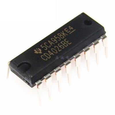
The IC CD4026 is an IC which can perform the function of both a counter as well a 7-segment Driver. One single IC can be used to count form zero (0) to nine (9) directly on a Common Cathode type 7-segment display. The count can be increased by simply giving a high clock pulse; also more than one digit (0-9) can be created by cascading more than one CD4026 IC. So if you have a 7-segment (CC) display on which you have to display numbers that are being counted based on some condition then this IC will be a perfect choice.
-
Features
- High Speed Operation: tpd (CLK to Y) = 20 ns typ (CL = 50 pF)
- High Output Current: Fanout of 10 LSTTL Loads
- Wide Operating Voltage: VCC = 2 V to 6 V
- Low Input Current: 1 µA max
- Low Quiescent Supply Current: ICC (static) = 4 µA max (Ta = 25°C)
-
-44%

74LS158 is a high speed Quad 2-input Multiplexer. It selects four bits of data from two sources using the common Select and Enable inputs.
-
-11%
CD4033 is a simple decoder IC that is commonly used to drive Seven segment displays.
-
-20%
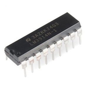
- Analog Controlled LED Driver IC
- Number of controllable LEDs: 10
- Operating Voltage: 3V to 18V
- Input Analog voltage range: 1.2V to 12V
- LED sink current: 2mA to 30mA (programmable)
- Both Dot/Bar mode available
- Can be cascaded to control upto 100 LEDs
- Available in 18-pin DIP package
-
-20%
2SA1941 bipolar transistor p-n-p type transistor. Collector-Emitter Voltage: -140 V Collector-Base Voltage: -140 V Emitter-Base Voltage: -5 V Collector Current: -10 A Collector Dissipation – 100 W DC Current Gain (hfe) – 55 to 160 Transition Frequency – 30 MHz Operating and Storage Junction Temperature Range -55 to +150 ?C
-
-51%

DS1302 is a tickle-charge timekeeping chip which contains a real-time clock/calendar and 31 bytes of static RAM. DS1302 uses serial communication to interact with microcontrollers. Also, it automatically adjust the date for the month with fewer days. Clock operates in 24hr or 12hr format with an AM/PM indicator. DS1302 chip is also commonly used as DS1302 RTC module which comes with a 32 kHz crystal and on-board battery backup all in a small SIP module that is compatible with a breadboard. DS1302 module are used by makers with Arduino, Raspberry Pi and other Micro-controllers.
-
-41%
- Technology Family: LS
- Rating: Catalog
- Supply voltage: 1.0V to 5.5V
- Frequency at nominal voltage: 35 MHz
- Typical propagation delay: 21nS
- Low power consumption: 32mW
- Operating temperature: -40ºC to +125ºC
- ESD protection
- Balanced propagation delays
- Designed specifically for high speed
- Channels (#): 1
- Configuration: 3:8
- Product type: Standard
-

- N-Channel Power MOSFET
- Continuous Drain Current (ID): 8A
- Gate threshold voltage (VGS-th) is 10V (limit = 20V)
- Drain to Source Breakdown Voltage: 500V
- Drain Source Resistance (RDS) is 0.85 Ohms
- Rise time and fall time is 23nS and 20nS
- Available in To-220 package
-
-53%

SG3525 / KA3525 PWM Controller IC in Pakistan
Original price was: ₨190.00.₨89.00Current price is: ₨89.00. Quick View- DUAL SOURCE/SINK OUTPUT DRIVERS
- LATCHING PWM TO PREVENT MULTIPLE PULSES
- PULSE-BY-PULSE SHUTDOWN
- INTERNAL SOFT-START
- 8 TO 35 V OPERATION
- 100 Hz TO 500 KHz OSCILLATOR RANGE
- 5.1 V REFERENCE TRIMMED TO 1 %
- ADJUSTABLE DEADTIME CONTROL
- INPUT UNDERVOLTAGE LOCKOUT WITH HYSTERESIS
- SEPARATE OSCILLATOR SYNC TERMINAL
-
-18%
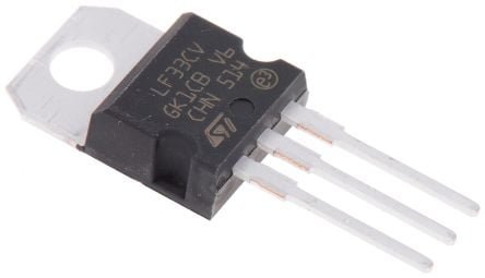
The LF33CV is a very low drop voltage regulator. It has an output voltage of 3.3 V and a output current of 500 mA. Input voltage range 2.5V to 16V. It is suitable for low noise, low power applications and specially in battery powered systems.
-

- Darlington medium-power NPN Transistor
- High DC Current Gain (hFE), typically 1000
- Continuous Collector current (IC) is 5A
- Collector-Emitter voltage (VCE) is 100 V
- Collector-Base voltage (VCB) is 100V
- Emitter Base Voltage (VBE) is 5V
- Base Current(IB) is 120mA
- Type NPN
- Collector-Emitter Voltage: 100V
- Collector-Base Voltage: 100V
- Emitter-Base Voltage: 5V
- Collector Current: 5A
- Collector Dissipation: 65W
- DC Current Gain (hfe): 1000
- Operating and Storage Junction Temperature Range: -65 to +150C
- Package: TO-220
-

IRF4905 MOSFET is a P-Channel HEXFET Power MOSFET available in a TO-220AB package and is based on Advanced Process Technology. It is mainly used for fast switching purpose, capable of providing ultra-low on-resistance. This tiny device comes with three terminals called gate, drain and source where the gate terminal is used to control the current on remaining two terminals. The area between source and drain is known as a channel that is widely dependent on the voltage applied to the gate terminal.
-
-34%

CD4538 – Dual Monostable Multivibrator
Original price was: ₨150.00.₨99.00Current price is: ₨99.00. Quick View- Wide supply voltage range 3.0V to 15V
- High noise immunity 0.45 VCC (typ.)
- Low power Fan out of 2 driving 74L TTL compatibility or 1 driving 74LS
- New formula: PWOUT e RC (PW in seconds, R in Ohms, C in Farads)
- g1.0% pulse-width variation from part to part (typ.) Wide pulse-width range 1 ms to %
- Separate latched reset inputs
- Symmetrical output sink and source capability
- Low standby current 5 nA (typ.) @ 5 VDC Y Pin compatible to CD4528
-
-18%

9N90 is a N-Channel enhancement mode power mosfet.
-

The 2N2905 from Multicomp Pro is a through-hole, silicon planar PNP low power bipolar transistors in a TO-39 metal can package. These are general-purpose transistors suitable for switching applications.
-
-46%
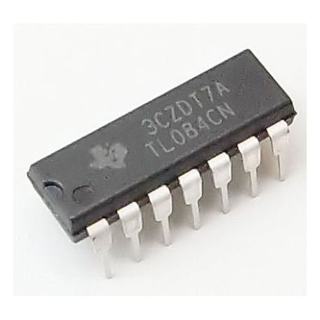
TL084 circuits JFET Input Op-amp
Original price was: ₨200.00.₨109.00Current price is: ₨109.00. Quick View- Input Offset Voltage Options of 6.0 mV and 15 mV Max
- Low Input Bias Current: 30 pA
- Low Input Offset Current: 5.0 pA
- Wide Gain Bandwidth: 4.0 MHz
- High Slew Rate: 13 V/s
- Low Supply Current: 1.4 mA per Amplifier
- High Input Impedance: 1012
-

The DS1307 serial real-time clock (RTC) is a lowpower, full binary-coded decimal (BCD) clock/calendar plus 56 bytes of NV SRAM. Address and data are transferred serially through an I2C, bidirectional bus. The clock/calendar provides seconds, minutes, hours, day, date, month, and year information. The end of the month date is automatically adjusted for months with fewer than 31 days, including corrections for leap year. The clock operates in either the 24-hour or 12-hour format with AM/PM indicator. The DS1307 has a built-in power-sense circuit that detects power failures and automatically switches to the backup supply. Timekeeping operation continues while the part operates from the backup supply.
-
-20%
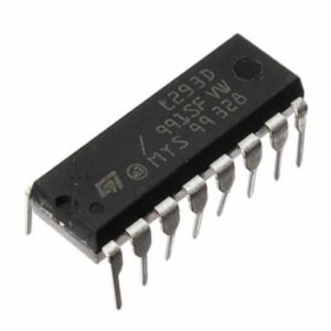
L293D L293-D Dual H-Bridge Motor Driver
Original price was: ₨150.00.₨120.00Current price is: ₨120.00. Quick View- Can drive 2 DC motors simultaneously in either direction
- Wide voltage supply range: 4.5V to 36V
- Separate input-logic supply
- Internal ESD protection
- High-noise-immunity inputs
- Thermal shutdown
- Output clamp diodes for inductive transient suppression