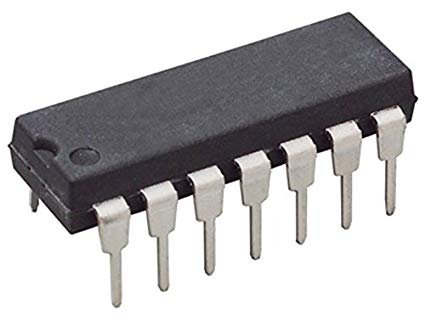
CD4073 Triple 3 Input AND Gate IC
CD4073 Triple 3 Input AND Gate IC made by using the complimentary MOS (CMOS) technology integrated with P and N type MOSFETS. This IC allows system designers to utilize the AND gate function and supplement the existing family of CMOS gates. The IC offers a wide array of workable voltages and conditions making it easy to use with different DLD configurations. The output of the IC is always available in TTL, allowing it to be easily interfaceable with CMOS, NMOS, and other TTL devices.
CD4073 Key Features
- High-Voltage Types (20V Rating)
- CD4073BMS Triple 3-Input AND Gate
- CD4081BMS Quad 2-Input AND Gate
- CD4082BMS Dual 4-Input AND Gate
- Medium Speed Operation: tPLH, tPHL = 60ns (typ) at VDD = 10V
- 100% Tested for Quiescent Current at 20V
- Maximum Input Current of 1A at 18V Over Full Package Temperature Range; 100nA at 18V and +25oC
SPECIFICATIONS:
- Triple 3 Input AND Gate
- No Of Inputs: 9
- No Of Outputs: 3
- Supply Voltage Range: 3 to 15V
- Quiescent Current Max.: 4A
- Propagation Delay Time Max.: 110ns
- Package: DIP-14
| Pin No | Pin Name | Description |
|---|---|---|
| 1 | A0 | Input Pin 0 of AND Gate 1 |
| 2 | A1 | Input Pin 1 of AND Gate 1 |
| 3 | B0 | Input Pin 0 of AND Gate 2 |
| 4 | B1 | Input Pin 1 of AND Gate 2 |
| 5 | B2 | Input Pin 2 of AND Gate 2 |
| 6 | Q1 | The output of AND Gate 2 |
| 7 | VSS | Source Supply |
| 8 | A2 | input pin 2 of AND Gate 1 |
| 9 | Q0 | The output of AND Gate 1 |
| 10 | Q2 | The output of AND Gate 3 |
| 11 | C0 | Input Pin 0 of AND Gate 3 |
| 12 | C1 | Input Pin 1 of AND Gate 3 |
| 13 | C2 | Input Pin 2 of AND Gate 3 |
| 14 | VDD | Drain Supply |
Application
- Measurement of frequency
- Enable gate and Inhibit gate
CD4073 Datasheet
You can download the datasheet for CD4073 Triple 3-input AND Gate


Reviews
There are no reviews yet.