-
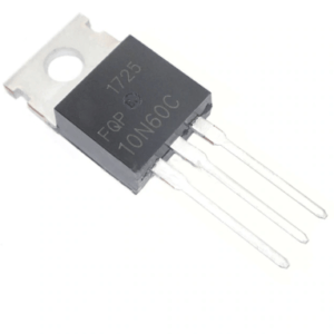
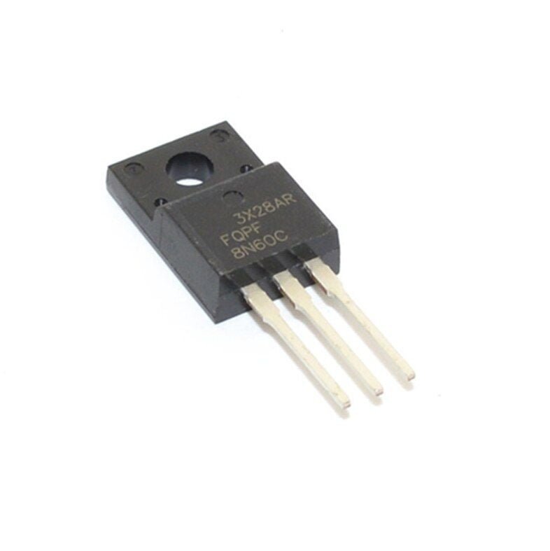
- Drain Current ID= 9.2A@ TC=25
- Drain Source Voltage : VDSS= 650V(Min)
- Static Drain-Source On-Resistance: RDS(on) = 0.83(Max)
- Avalanche Energy Specified
- Fast Switching
- Simple Drive Requirements
-
20N60 belongs to the family of N-channel MOSFET. Its basically a power MOSFET that means it can handle certain levels of power. Its working principle is based on UTC technology. It provides the fast switching application and the minimum on state resistance as well. handling of high current, high speed of switching and low on sate resistance are its major features. Its real life applications include servo motor drivers, UPS, speed control of AC motor and many more.
-
-37%

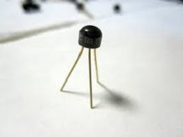
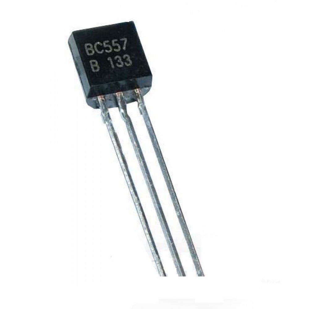
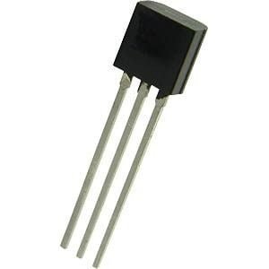
- Small Signal NPN Transistor
- Current Gain (hFE), typically 50 for small signal
- Continuous Collector current (IC) is 800mA
- Collector-Emitter voltage (VCEO) is 50 V
- Collector-Base voltage (VCB0) is 75V
- Emitter Base Voltage (VBE0) is 6V
- Turn on time is 40ns
- Turn off time is 250ns
- Available in To-92 Package
-

The 2N2905 from Multicomp Pro is a through-hole, silicon planar PNP low power bipolar transistors in a TO-39 metal can package. These are general-purpose transistors suitable for switching applications.
-

Features and Technical Specification
- Having a high value of current (max. 600 mA)
- Low voltage value (max. 40 V)
- It comes in different types of packages TO-92, TO-18
- These are Lead (Pb) free devices
- Collector to Emitter voltage (VCEO) is 40v (max.)
- Collector to Base voltage (VCBO) is 60v (max.)
- Emitter to Base voltage(VEBO) is 5v (normally)
- The maximum value of Collector current is 600mA
- Power dissipation at ambient temperature is about 400mW
- Having DC current gain (hfe) of 100 to 300 (max.)
- The temperature of operation and storage is -65 to +150 C
-
- Bi-Polar NPN Transistor
- DC Current Gain (hFE) is 300 maximum
- Continuous Collector current (IC) is 200mA
- Base- Emitter Voltage (VBE) is 6V
- Collector-Emitter Voltage (VCE) is 40V
- Collector-Base Voltage (VCB) is 60V
- Available in To-92 Package
-
- Bi-Polar PNP Transistor
- DC Current Gain (hFE) is 300 maximum
- Continuous Collector current (IC) is 200mA
- Emitter Base Voltage (VBE) is 5V
- Base Current(IB) is 5mA maximum
- Collector Emitter Voltage (VCE) is 40V
- Collector Base Voltage (VCB) is 40V
- Available in To-92 Package
-
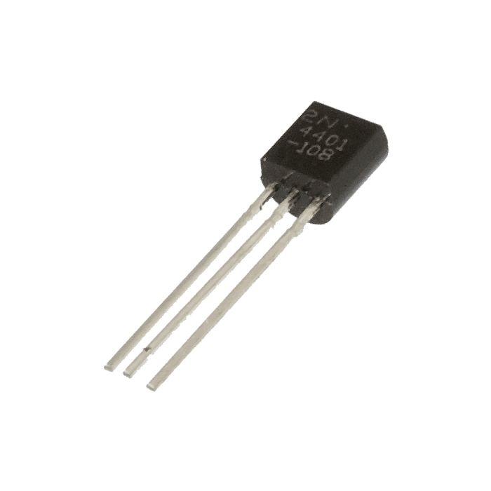
2N4401 is an NPN bipolar junction transistor that is mainly designed for general purpose, small signal, and switching applications.
-
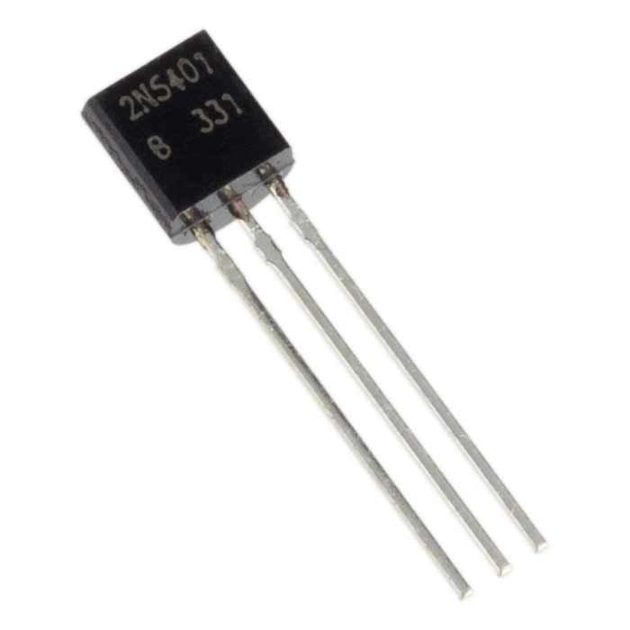
2N5401 Features and Electrical Characteristics
- Available in Pb Free package
- High collector breakdown voltage
- With DC Current Gain (hFE) up to 100
- Maximum voltage across collector and emitter: 150V
- Maximum current allowed trough collector: 600mA
- Maximum voltage across collector and base: 160 V
- Maximum voltage across base and emitter: 5V
- Operating temperature range: -55C to +150C
- Maximum power dissipation: 0.62 W
-
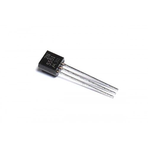
2N5551 is an NPN amplifier Transistor with an amplification factor (hfe) of 80 when the collector current is 10mA. The transistor is commonly used for amplification of audio or other low power signals.
-
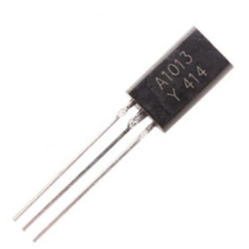
- Type Designator: 2SA1013
- Material of transistor: Si
- Polarity: PNP
- Maximum collector power dissipation (Pc), W: 0.9
- Maximum collector-base voltage Ucb, V: 160
- Maximum collector-emitter voltage Uce, V: 160
- Maximum emitter-base voltage Ueb, V: 6
- Maximum collector current Ic max, A: 2
- Maksimalna temperatura (Tj), °C: 125
- Transition frequency (ft), MHz: 15
- Collector capacitance (Cc), pF: 35
- Forward current transfer ratio (hFE), min: 60
- Noise Figure, dB: –
-
-20%
2SA1941 bipolar transistor p-n-p type transistor. Collector-Emitter Voltage: -140 V Collector-Base Voltage: -140 V Emitter-Base Voltage: -5 V Collector Current: -10 A Collector Dissipation – 100 W DC Current Gain (hfe) – 55 to 160 Transition Frequency – 30 MHz Operating and Storage Junction Temperature Range -55 to +150 ?C
-
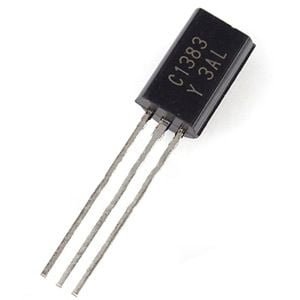
C1383 is a Bipolar NPN type transistor which is used for low-frequency power amplification and driver amplification.
-
-46%
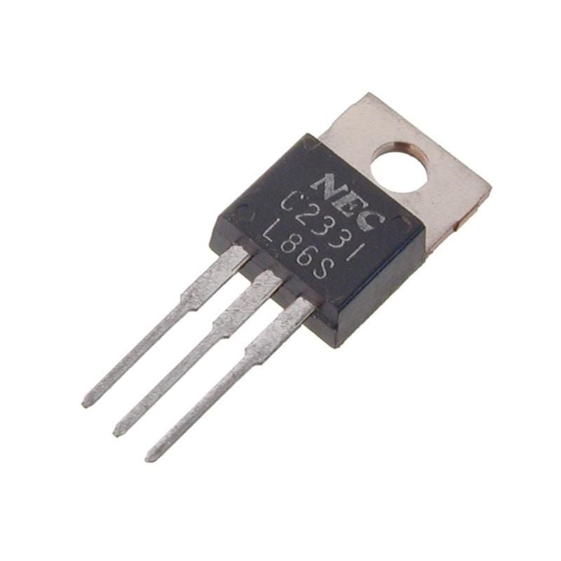
- Type Designator: 2SC2331
- Material of transistor: Si
- Polarity: NPN
- Maximum collector power dissipation (Pc), W: 1
- Maximum collector-base voltage |Ucb|, V: 80
- Maximum collector-emitter voltage |Uce|, V: 60
- Maximum emitter-base voltage |Ueb|, V: 8
- Maximum collector current |Ic max|, A: 0.7
- Transition frequency (ft), MHz: 30
- Collector capacitance (Cc), pF: 8
- Forward current transfer ratio (hFE), min: 40
- Noise Figure, dB: –
- Package of 2SC2331 transistor: TO92
-
-14%

- Type –NPN
- Collector-Emitter Voltage: 400V
- Collector-Base Voltage: 450V
- Emitter-Base Voltage: 7V
- Collector Current: 10A
- Collector Dissipation – 80W
- DC Current Gain (hfe) – 10
- Operating and Storage Junction Temperature Range -55 to +150C
-
-14%

- Type: NPN
- Collector-Emitter Voltage, max: 140 V
- Collector-Base Voltage, max: 140 V
- Emitter-Base Voltage, max: 5 V
- Collector Current − Continuous, max: 10 A
- Collector Dissipation: 100 W
- DC Current Gain (hfe): 55 to 160
- Transition Frequency, min: 30 MHz
- Operating and Storage Junction Temperature Range: -55 to +150 °C
- Package: TO-3P
-

- Type – NPN
- Collector-Emitter Voltage: 25 V
- Collector-Base Voltage: 30 V
- Emitter-Base Voltage: 7 V
- Collector Current: 0.05 A
- Collector Dissipation – 0.4 W
- DC Current Gain (hfe) – 130 to 520
- Transition Frequency – 220 MHz
- Noise Figure – 6 dB
- Operating and Storage Junction Temperature Range -55 to +150 °C
- Package – TO-92
-
-25%
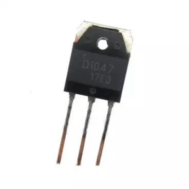
2SD1047 Bipolar NPN type Transistor.
-

- Type –NPN
- Collector-Emitter Voltage: 60V
- Collector-Base Voltage: 60V
- Emitter-Base Voltage: 5V
- Collector Current: 3A
- Collector Dissipation – 30W
- DC Current Gain (hfe) –40 to 320
- Transition Frequency – 5 MHz
- Operating and Storage Junction Temperature Range -55 to +150C
-
- 8N60 N-Channel Power Mosfet Transistor
- Ultra low gate charge ( typical 28 nC )
- Low reverse transfer capacitance ( Crss= typical 12.0 pF )
- Fast switching capability
- Avalanche energy specified
- Improved dv/dt capability, high ruggedness
- Drain Current: ID= 7.5A at TC= 25
- Drain Source Voltage: VDSS= 600V
- Static Drain-Source On-Resistance: RDS(on)< 1.2
-
-18%

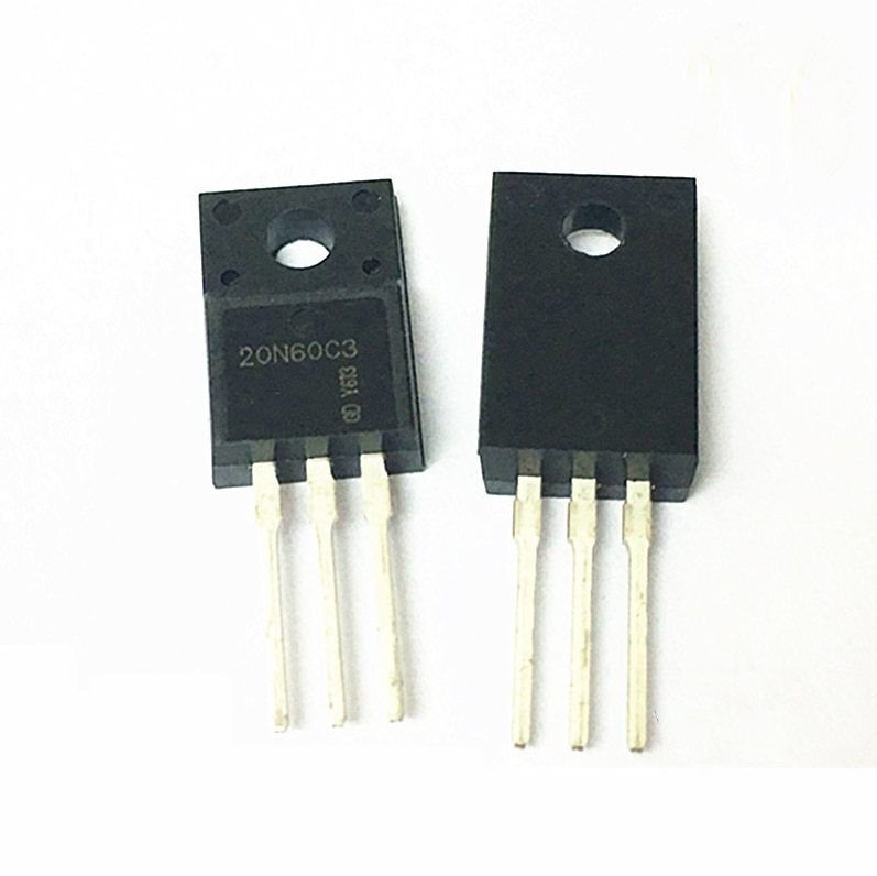
9N90 is a N-Channel enhancement mode power mosfet.
-

The main use is for audio frequency amplifier applications. It can also be used for the switching purpose just like other PNP transistors. When use as an Audio frequency general purpose amplifier, can be operated in the active region. This transistor is further divided into four groups according to the DC current gain, O, Y, G, and L and has 140, 240, 400 and 700 hfe DC current gain respectively.
-
-28%

- Small Signal NPN Transistor
- Current Gain (hFE): 450 (maximum)
- Continuous Collector current (IC) is 100mA
- Collector-Emitter voltage (VCEO) is 45V
- Collector-Base voltage (VCB0) is 50V
- Emitter Base Voltage (VBE0) is 6V
- Available in To-18 Metal can Package
-

- Bi-Polar NPN Transistor
- DC Current Gain (hFE) is 900 maximum
- Continuous Collector current (IC) is 200mA
- Emitter Base Voltage (VBE) is 5V
- Base Current(IB) is 10mA maximum
- Available in TO-18 Metal Can Package
- Maximum Collector-Base Voltage |Vcb|: 30 V’
- Collector Dissipation: 0.3 W
- Transition Frequency:150 MHz
- Operating Junction Temperature Max (Tj): 175 °C
- Noise Figure – 2 dB
- Operating and Storage Junction Temperature Range -65 to +175 °C
- Collector Capacitance 5pF
-

BC109 is a bipolar NPN type transistor. It has Collector-Emitter Volt (Vceo): 20V & Collector Current (Ic): 0.2A.
-
BC134 is a NPN type transistor. Its Maximum Collector-Base Voltage |Vcb|: 45 V & Maximum Collector Current |Ic max|: 0.2 A.
-

BC327 is a PNP bipolar junction transistor which is mainly designed for general purpose, small signal and switching applications.
-
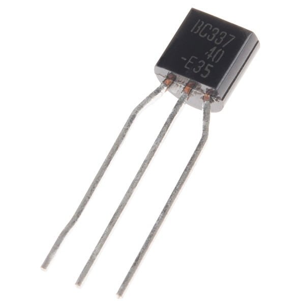
This is the BC337, an NPN silicon BJT (Bipolar Junction Transistor). This little transistor can help in your project by being used to help drive large loads or amplifying or switching applications. The BC337 is specifically rated at 50V and 800mA max.
-
- Bi-Polar NPN Transistor
- DC Current Gain (hFE) is 800 maximum
- Continuous Collector current (IC) is 500mA
- Emitter Base Voltage (VBE) is 5V
- Base Current(IB) is 5mA maximum
- Available in To-92 Package
-
- Package Type: TO-92
- Transistor Type: PNP
- Max Collector Current(IC): -100mA
- Max Collector-Emitter Voltage (VCE): -45V
- Max Collector-Base Voltage (VCB): -50V
- Max Emitter-Base Voltage (VBE): -5V
- Max Collector Dissipation (Pc): 500 Milliwatt
- Max Transition Frequency (fT): 100 MHz
- Minimum & Maximum DC Current Gain (hFE): 125 to 800
- Max Storage & Operating temperature Should be: -65 to +150Centigrade
-
- Plastic casing NPN Transistor
- Continuous Collector current (IC) is 1.5A
- Collector-Emitter voltage (VCE) is 80 V
- Collector-Base voltage (VCB) is 80V
- Base Current (Ib) is 0.5A
- Emitter Base Breakdown Voltage (VBE) is 5V
- DC current gain (hfe) is 40 to 160
- Available in To-225 package
-
- Bi-Polar PNP Transistor
- Continuous Collector current (IC) is -1.5A
- Collector-Emitter voltage (VCE) is- 80 V
- Collector-Base voltage (VCB) is- 80V
- Base Current (Ib) is -0.5A
- Emitter Base Breakdown Voltage (VBE) is -5V
- DC current gain (hfe) is 40 to 160
- Available in To-225 and SOT-32 Package
- Collector Dissipation: 12.5 W
- Operating Junction Temperature Max (Tj): 150°C
-

- HF applications in radio and television receivers
- FM tuners
- Low noise AM mixer-oscillators
- IF amplifiers in AM/FM receivers
-
- Package Type: TO-92
- Transistor Type: NPN
- Max Collector Current(IC): 30mA
- Max Collector-Emitter Voltage (VCE): 20V
- Max Collector-Base Voltage (VCB): 30V
- Max Emitter-Base Voltage (VBE): 5V
- Max Collector Dissipation (Pc): 300 Milliwatt
- Max Transition Frequency (fT): 120 MHz
- Minimum & Maximum DC Current Gain (hFE): 35 to 125
- Max Storage, Operating & Junction temperature range: -65 to +150 Centigrade
-
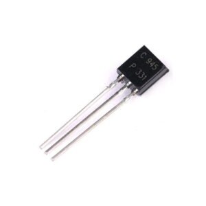
- 2sc925 well known as C945 NPN transistor.
- Max Voltage Collector Emmiter=50 V.
- Max Collector current=150 mA.
- Collector power dissipation: 400 mW.
- Japanese High-frequency amplifier NPN Transistor.
- Current Gain (hFE) is 70 to 700 (high linearity).
- Continuous Collector current (IC) is 150mA.
- Collector-Emitter voltage (VCEO) is 50 V.
- Collector-Base voltage (VCB0) is 60V.
- Emitter Base Voltage (VBE0) is 5V.
- Transition Frequency is 150MHz.
-
-26%

512 bits Electrically Programmable Read Only Memory (EPROM) communicates with the economy of one signal plus ground
. Unique, factory-lasered and tested 64-bit registration number (8-bit family code + 48-bit serial number + 8-bit CRC tester) assures absolute traceability because no two parts are alike
. Built-in multidrop controller ensures compatibility with other MicroLAN products
. EPROM partitioned into two 256-bit pages for randomly accessing packetized data
. Each memory page can be permanently write-protected to prevent tampering
. Device is an “add-only” memory where additional data can be programmed into EPROM without disturbing existing data
. Architecture allows software to patch data by superseding an old page in favor of a newly programmed page
. Reduces control, address, data, power, and programming signals to a single data pin
. Directly connects to a single port pin of a microprocessor and communicates at up to 16.3 kbps
. 8-bit family code specifies DS2501 communications requirements to reader
-
- Package Type: TO-220
- Transistor Type: N Channel
- Max Voltage Applied From Drain to Source: 55V
- Max Gate to Source Voltage Should Be: 20V
- Max Continues Drain Current is : 49A
- Max Pulsed Drain Current is: 160A
- Max Power Dissipation is: 94W
- Minimum Voltage Required to Conduct: 2V to 4V
- Max Storage & Operating temperature Should Be: -55 to +170 Centigrade
-
-38%

- N-Channel Power MOSFET
- Continuous Drain Current (ID) is 110A when VGS is 10V
- Minimum Gate threshold voltage 2V
- Drain to Source Breakdown Voltage: 55V
- Low On-Resistance of 8.0m
- Gate-Source Voltage is (VGS) is 20V
- Rise time is 101ns
- It is commonly used with Power Switching circuits
- Available in To-220 package
-

IRF4905 MOSFET is a P-Channel HEXFET Power MOSFET available in a TO-220AB package and is based on Advanced Process Technology. It is mainly used for fast switching purpose, capable of providing ultra-low on-resistance. This tiny device comes with three terminals called gate, drain and source where the gate terminal is used to control the current on remaining two terminals. The area between source and drain is known as a channel that is widely dependent on the voltage applied to the gate terminal.
-
- Fast Switching Applications
- Uninterruptible Power Supplies
- Battery Chargers
- Battery Management Systems
- Solar Battery Chargers
- Solar Uninterruptible Power Supplies
- Motor Driver Applications
- Telecommunication Applications
- Computer Related Applications
-

N-Channel Power MOSFET provide the circuit designer with the best combination of fast switching, ruggedized device design, low on-resistance and cost-effectiveness.
-

- Dynamic dV/dt rating
- Repetitive avalanche rated
- Fast switching
- Ease of paralleling
- Simple drive requirements
-

- N-Channel Power MOSFET
- Continuous Drain Current (ID): 10A
- Gate threshold voltage (VGS-th) is 10V (limit = 20V)
- Drain to Source Breakdown Voltage: 400V
- Drain Source Resistance (RDS) is 0.55 Ohms
- Rise time and fall time is 27nS and 24nS
- Available in To-220 package
-

This Power MOSFET provides the circuit designer with the best combination of fast switching, ruggedized device design, low on-resistance and cost-effectiveness.
-

- N-Channel Power MOSFET
- Continuous Drain Current (ID): 8A
- Gate threshold voltage (VGS-th) is 10V (limit = 20V)
- Drain to Source Breakdown Voltage: 500V
- Drain Source Resistance (RDS) is 0.85 Ohms
- Rise time and fall time is 23nS and 20nS
- Available in To-220 package
-
-15%
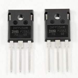
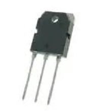
IRFP250 N-channel Power MOSFET
Original price was: ₨280.00.₨239.00Current price is: ₨239.00. Quick View- Repetitive Avalanche Ratings
- Dynamic dv/dt Rating
- Hermetically Sealed
- Simple Drive Requirements
- Ease of Paralleling
- Type Designator: IRF250
- Type of Transistor: MOSFET
- Type of Control Channel: N -Channel
-
-38%

MOSFET (metal-oxide-semiconductor field-effect transistor, pronounced MAWS-feet) is a special type of field-effect transistor (FET) that works by electronically varying the width of a channel along which charge carriers (electrons or holes) flow. The wider the channel, the better the device conducts. The charge carriers enter the channel at the source and exit via the drain. The width of the channel is controlled by the voltage on an electrode called the gate, which is located physically between the source and the drain and is insulated from the channel by an extremely thin layer of metal oxide.
-
-20%
 Out Of Stock
K2045 Mosfet 2SK2045 TO-220F FET K2045 NPN
Original price was: ₨50.00.₨40.00Current price is: ₨40.00. Quick ViewLow ON resistance. Ultrahigh-speed switching. High-speed diode built in.
-
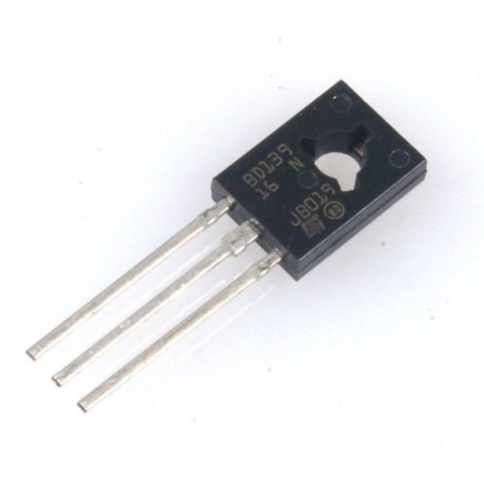
This NPN Bipolar Darlington Transistor is designed for use in switching applications, such as print hammer, relay, solenoid and lamp drivers.
-
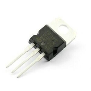
TIP122 transistor designed for general purpose amplifier and low speed switching applications.
-

- Darlington medium-power NPN Transistor
- High DC Current Gain (hFE), typically 1000
- Continuous Collector current (IC) is 5A
- Collector-Emitter voltage (VCE) is 100 V
- Collector-Base voltage (VCB) is 100V
- Emitter Base Voltage (VBE) is 5V
- Base Current(IB) is 120mA
- Type NPN
- Collector-Emitter Voltage: 100V
- Collector-Base Voltage: 100V
- Emitter-Base Voltage: 5V
- Collector Current: 5A
- Collector Dissipation: 65W
- DC Current Gain (hfe): 1000
- Operating and Storage Junction Temperature Range: -65 to +150C
- Package: TO-220
-

The Bipolar Power Transistor is designed for use in general purpose amplifier and switching applications.
-

- Low saturation voltage
- Simple drive requirements
- High safe operating area
- For low distortion complementary designs
- Easy to carry and handle
-
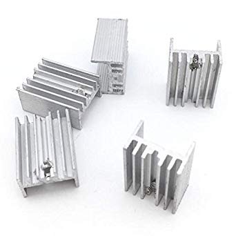
A heat-sink is designed to remove heat from a transistor and dissipate it into the surrounding air as efficiently as possible. Heat-sinks take many different forms, such as finned aluminium or copper sheets or blocks, often painted or anodised matt black to help dissipate heat more quickly. Good physical contact between the transistor and heat-sink is essential, and a heat transmitting grease (heat-sink compound) is smeared on the contact area before clamping the transistor to the heat-sink.
-
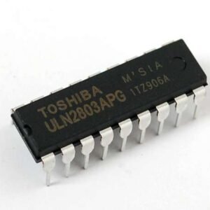
ULN 2803 is a high-voltage, high-current Darlington transistor array. The device consists of eight npn Darlington pairs that feature high-voltage outputs with common-cathode clamp diodes for switching inductive loads. The collector-current rating of each Darlington pair is 500 mA. The Darlington pairs may be connected in parallel for higher current capability. Applications include relay drivers, hammer drivers, lamp drivers, display drivers (LED and gas discharge), line drivers, and logic buffers.
-
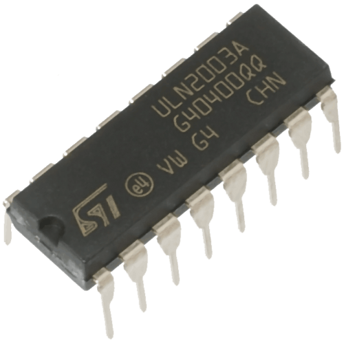
- Seven Darlingtons per package
- Output current 500 mA per driver (600 mA peak)
- Output voltage 50 V
- Integrated suppression diodes for inductive loads
- Outputs can be paralleled for higher current
- TTL/CMOS/PMOS/DTL compatible inputs
- Inputs pinned opposite outputs to simplify