-
-53%

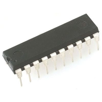
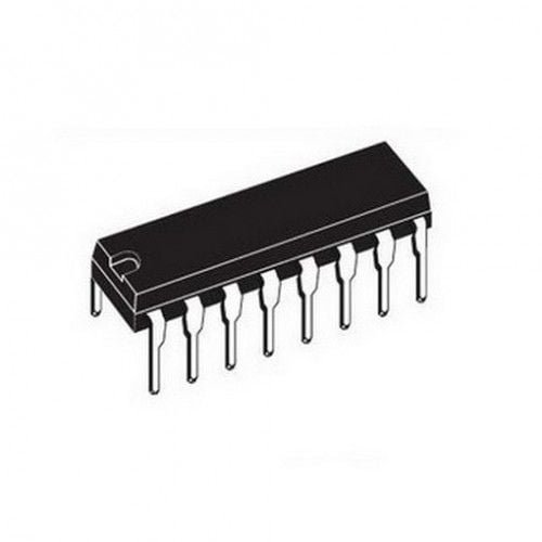
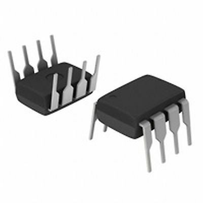
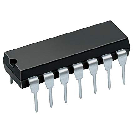
SG3525 / KA3525 PWM Controller IC in Pakistan
Original price was: ₨190.00.₨89.00Current price is: ₨89.00. Quick View- DUAL SOURCE/SINK OUTPUT DRIVERS
- LATCHING PWM TO PREVENT MULTIPLE PULSES
- PULSE-BY-PULSE SHUTDOWN
- INTERNAL SOFT-START
- 8 TO 35 V OPERATION
- 100 Hz TO 500 KHz OSCILLATOR RANGE
- 5.1 V REFERENCE TRIMMED TO 1 %
- ADJUSTABLE DEADTIME CONTROL
- INPUT UNDERVOLTAGE LOCKOUT WITH HYSTERESIS
- SEPARATE OSCILLATOR SYNC TERMINAL
-
-40%
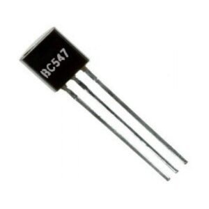

BC547-B166 NPN Transistor 50V/ 0.3A
Original price was: ₨15.00.₨9.00Current price is: ₨9.00. Quick ViewOverall, the BC547 NPN transistor is a versatile and reliable transistor that is suitable for a wide range of applications. NPN Transistor BC547 is a popular choice for electronic hobbyists and engineers because it is inexpensive and easy to use. here are the specifications of the BC547-B166 NPN transistor:
- Collector current (maximum): 300mA
- Collector-emitter voltage (maximum): 65V
- Base current (maximum): 5mA
- Current gain (hFE): 110 to 800
- Package: TO-92
-
-27%
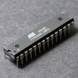
Atmega8 Microcontrollers IC 8Kbytes
Original price was: ₨899.00.₨659.00Current price is: ₨659.00. Quick ViewThe Atmel AVR ATmega8 is a low-power CMOS 8-bit microcontroller based on the AVR RISC architecture. By executing powerful instructions in a single clock cycle, the ATmega8 achieves throughputs approaching 1MIPS per MHz, allowing the system designer to optimize power consumption versus processing speed.
-
-30%
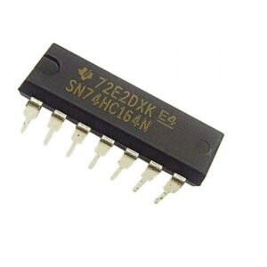
74HC164 8-Bit Parallel-Out Shift Register
Original price was: ₨100.00.₨70.00Current price is: ₨70.00. Quick ViewFeatures/Specs:
Wide Supply Voltage Range from 2.0V to 6.0V
Sinks or Sources 4mA at VCC = 4.5V
CMOS Low Power Consumption
Schmitt Trigger Action at all Inputs
ESD Protection Exceeds JESD 22v 200-V Machine Model (A115)
2000-V Human Body Model (A114)
Exceeds 1000-V Charged Device Model (C101)
Range of Package Options SO-14 and TSSOP-14
Totally Lead-Free & Fully RoHS Compliant
Halogen and Antimony Free. Green Device
-
-33%
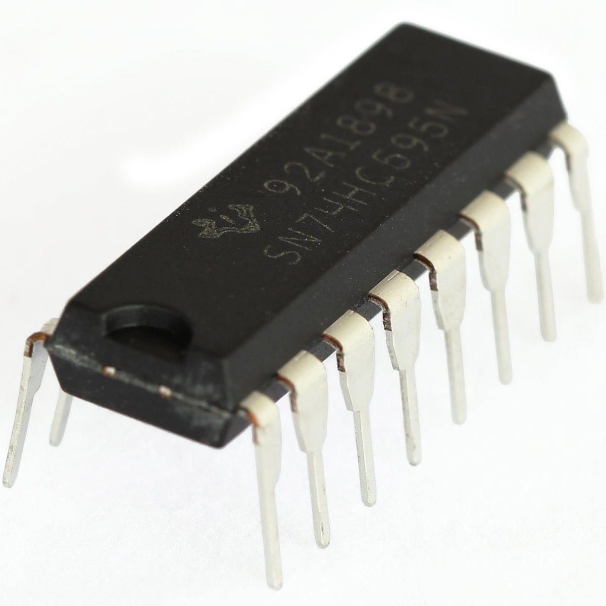
74HC595 74HC595D Shift Register
Original price was: ₨60.00.₨40.00Current price is: ₨40.00. Quick View74HC595 8-BIT SERIAL-IN SERIAL OR PARALLEL-OUT SHIFT REGISTER contain an 8-bit serial-in, parallel-out shift register that feeds an 8-bit D-type storage register. The storage register has parallel 3-state outputs. Separate clocks are provided for both the shift and storage register. The shift register has a direct overriding clear (SRCLR) input, serial (SER) input, and serial outputs for cascading. When the output-enable (OE) input is high, the outputs are in the high-impedance state.
-
-33%

D-Type Flip-Flop 74HC175 DIP16 – SN74HC175N
Original price was: ₨60.00.₨40.00Current price is: ₨40.00. Quick View- Outputs can drive up to 10 LSTTL loads
- Contain four flip-flops with double-rail outputs
- 80A Maximum low power consumption
- 13ns Typical tpd
- 4mA Output drive at 5V
- 1A Maximum low input current
-
-33%
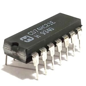
CD74HC21E 74HC21 Dual 4-Input Positive-AND Gates IC
Original price was: ₨60.00.₨40.00Current price is: ₨40.00. Quick View- Wide Operating Voltage Range of 2 V to 6 V
- Outputs Can Drive Up To 10 LSTTL Loads
- Low Power Consumption, 20-?A Max ICC
- Typical tpd= 11 ns
- ?4-mA Output Drive at 5 V
- Low Input Current of 1 ?A Max
-
-8%
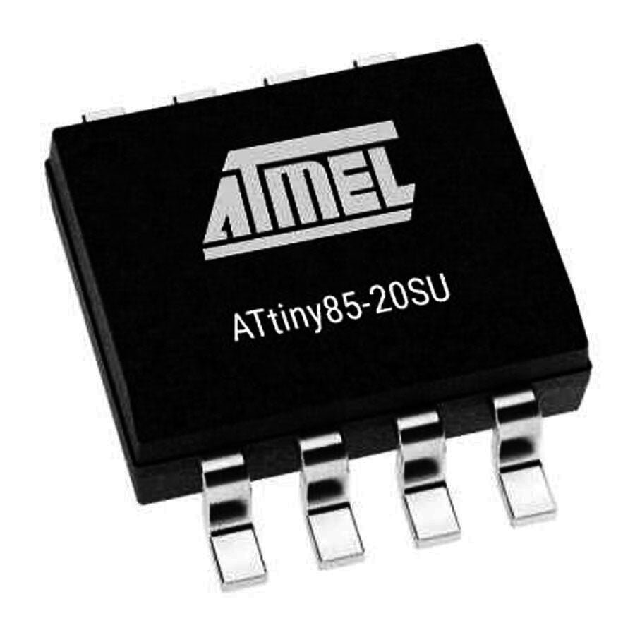
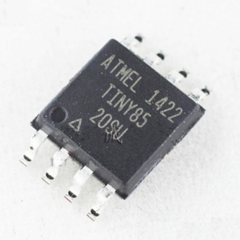
Atmel Attiny85 Attiny-85 ATtiny85-20PU
Original price was: ₨1,200.00.₨1,099.00Current price is: ₨1,099.00. Quick ViewFeatures of ATtiny85 Microcontroller:-
- Flash (Kbytes): 8 Kbytes
- Pin Count: 8
- Max. Operating Freq. (MHz): 20 MHz
- CPU: 8-bit AVR
- Number of Touch Channels: 3
- Hardware QTouch Acquisition: No
- Max I/O Pins: 6
- Ext Interrupts: 6
- USB Interface:No
- Package – SMD
-
-20%
 Out Of Stock
 -

The CD4040 is a 12-stage ripple carry binary counter. The counters are advanced one count on the negative transition of each clock pulse. The counters are reset to the zero state by a logical 1 at the reset input independent of the clock.
-

The 4072 is a member of the 4000 Series CMOS range, and contains two independent OR gates, each with four inputs.
-
This is a monostable multivibrator or pulse generator.
-

74HC540 is a 20 Pin Octal 3-state Inverting Buffer IC having 2V to 6V Operating Voltage range with 6mA output current. The 3-STATE buffers utilize advanced silicon-gate CMOS technology. They possess high drive current outputs which enable high speed operation even when driving large bus capacitances.
-
The 74LS373 consists of eight latches with 3-state outputs for bus organized system applications. The flip-flops appear transparent to the data.
-

The 7408 is a QUAD 2-Input AND gates and contains four independent gates each of which performs the logic AND function. It comes in 14-pin DIP package. 7408 AND Gate IC 74HC244 74244 Octal Buffers & Line Driver IC in Pakistan
-

The SN74HC244N is an Octal Buffer and Line Driver IC, designed specifically to improve both the performance and density of 3-state memory address drivers, clock drivers and bus-oriented receivers and transmitters. This device organized as two 4-bit buffers/drivers with separate output-enable (OE)/inputs. When OE/ is low, the device passes non-inverted data from the A inputs to the Y outputs. When OE/ is high, the outputs are in the high-impedance state.
-
Texas Instruments SN7414 Series Inverters are available at ElectroNation.
-
The 74LS139 is a high speed Dual 1-of-4 Decoder/De-multiplexer. The device has two independent decoders, each accepting two inputs and providing four mutually exclusive active LOW Outputs. Each decoder has an active LOW Enable input which can be used as a data input for a 4-output demultiplexer. Each half of the LS139 can be used as a function generator providing all four minterms of two variables. The LS139 is fabricated with the Schottky barrier diode process for high speed and is completely compatible with all Motorola TTL families.
-
This IC is a 16-Bit SPI I/O Expander with Serial Interface. This IC has 25mA sink/source capability per I/O.
-
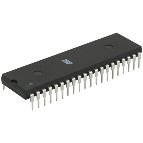
8051 is an 8-bit family of microcontrollers developed by Intel. This microcontroller was also referred as a system on a chip because it has 128 bytes of RAM, 4K bytes of ROM, 2 Timers, 1 Serial port, and four ports on a single chip. The CPU can work for only 8 bits of data at a time because 8051 is an 8-bit processor. In case the data is larger than 8 bits then it has to be broken into parts so that the CPU can process conveniently.
-
-13%
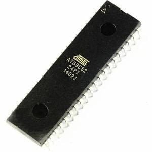
The AT89C52 is a lowe power, high performance CMOS 8-bit microcontroller with 8K bytes of Flash programmable and reaseable read only memory (PEROM). The on-chip flash allows the program memory to be reprogrammed in-syetem.
-
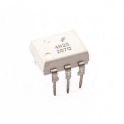
The 4N25 is an optocoupler for general purpose applications. It contains a light emitting diode optically coupled to a photo-transistor.
-
-12%
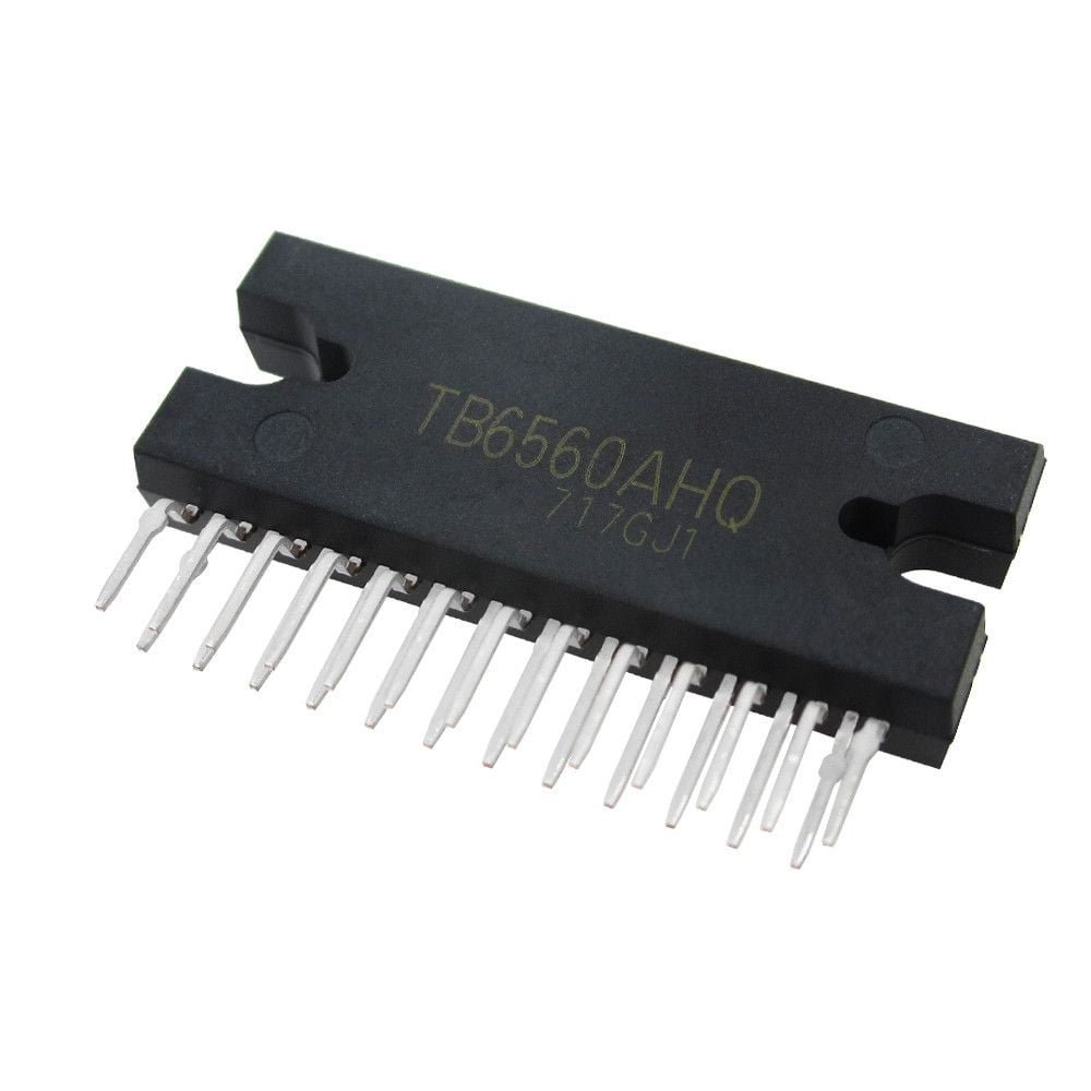
TB6560 Stepper Motor Driver IC
Original price was: ₨1,050.00.₨929.00Current price is: ₨929.00. Quick ViewThe latest 3rd generation TB6565 Stepper Driver has been upgraded to the intelligent, professional and industrial-level drive, embedding intelligent memory chip and upgrading the external manual control tools.
-
-34%

IR2110 Mosfet & IGBT Gate Driver IC
Original price was: ₨450.00.₨299.00Current price is: ₨299.00. Quick ViewThe IR2110 is high voltage, high speed power MOSFET and IGBT drivers with independent high and low side referenced output channels.
-
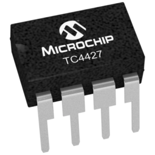
TC 4427 is a dual high speed power mosfet driver. ThIS device IS highly latch-up resistant under any conditions within their power and voltage ratings. All terminals are fully protected against Electrostatic Discharge (ESD).
-
-11%
CD4033 is a simple decoder IC that is commonly used to drive Seven segment displays.
-

It is an integrated circuit that converts the signals from the RS232 serial port to the proper signal which is used in the TTL compatible digital logic circuits. The MAX232 can convert the signals like RX, TX, CTS, and RTS and it is a dual driver/receiver.
-
The Exclusive OR gates are monolithic complementary MOS (CMOS) integrated circuits constructed with N-Channel and P-Channel enhancement mode transistors. All inputs are protected against static discharge with diodes to VDD and VSS.
-
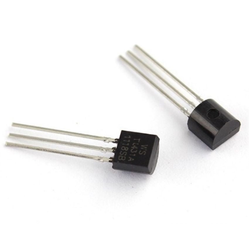
The TL431 is three-terminal adjustable shunt regulators, with specified thermal stability over applicable automotive, commercial, and military temperature ranges. The output voltage can be set to any value between Vref (approximately 2.5 V) and 36 V, with two external resistors. These devices have a typical output impedance of 0.2 .
-
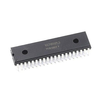
- Guaranteed zero reading for 0 V input on all scales
- True polarity at zero for precise null detection
- 1pA typical input current
- True differential input and reference, direct display drive – LED lCL7107
- Low noise – less than 15 VP-P
- On-chip clock and reference
- Low power dissipation – typically less than 10mW
- No additional active circuits required
- Enhanced display stability
- Pb-free (RoHS compliant)
-
This device is designed for use where the output voltage is a product of an input voltage (signal) and a switching function (carrier). Typical applications include suppressed carrier and amplitude modulation, synchronous detection, FM detection, phase detection, and chopper applications.
-
-28%
74LS47 IC – Common Anode LED Driver
Original price was: ₨90.00.₨65.00Current price is: ₨65.00. Quick View74LS47 is a BCD to 7-segment decoder/driver IC. It accepts a binary coded decimal as input and converts it into a pattern to drive a seven-segment for displaying digits 0 to 9.
-
-20%
 Out Of Stock
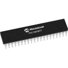
PIC 16F877 Microcontroller
Original price was: ₨1,500.00.₨1,199.00Current price is: ₨1,199.00. Quick ViewThis robust (200 nanosecond instruction execution) yet easy-to-program (only 35 single word instructions) CMOS FLASH-based 8-bit microcontroller packs Microchip’s robust PIC® architecture into a 40- or 44-pin package. It is upwards compatible with the PIC16C5X, PIC12CXXX and PIC16C7X devices. The PIC16F877A features 256 bytes of EEPROM data memory, self-programming, an ICD, 2 Comparators, 8 channels of 10-bit Analog-to-Digital (A/D) converter, 2 capture/compare/PWM functions, the synchronous serial port can be configured as either 3-wire Serial Peripheral Interface (SPI™) or the 2-wire Inter-Integrated Circuit (I²C™) bus and a Universal Asynchronous Receiver Transmitter (USART). These features make it ideal for more advanced level A/D applications in automotive, industrial, appliances and consumer applications.
-

ULN2004 Features
- Output current (single output): 500mA (MAX.)
- High sustaining voltage output: 50V (MIN.)
- Output clamp diodes
- Inputs compatible with various types of logic
-
-44%

74LS158 is a high speed Quad 2-input Multiplexer. It selects four bits of data from two sources using the common Select and Enable inputs.
-
Features
- High Speed Operation: tpd (CLK to Y) = 20 ns typ (CL = 50 pF)
- High Output Current: Fanout of 10 LSTTL Loads
- Wide Operating Voltage: VCC = 2 V to 6 V
- Low Input Current: 1 µA max
- Low Quiescent Supply Current: ICC (static) = 4 µA max (Ta = 25°C)
-
-20%
8051 Atmel AT89C51 Microcontroller 8-bit
Original price was: ₨500.00.₨399.00Current price is: ₨399.00. Quick View- Compatible with MCS-51 Products
- 4K Bytes of In-System Reprogrammable Flash Memory
- Endurance: 1,000 Write/Erase Cycles
- Fully Static Operation: 0 Hz to 24 MHz
- Three-Level Program Memory Lock
- 128 x 8-Bit Internal RAM
- 32 Programmable I/O Lines
- Two 16-Bit Timer/Counters
- Six Interrupt Sources
- Programmable Serial Channel
- Low Power Idle and Power Down Modes
-
-8%

This Tri-state bi-directional transceiver utilize advanced silicon-gate CMOS technology and is intended for two-way asynchronous communication between data buses. They have high drive current outputs which enable high speed operation even when driving large bus capacitances. The circuit possess the low power consumption of CMOS circuitry, yet have speeds comparable to low power Schottky TTL circuits.
-
-9%
- Internally frequency compensated for unity gain
- Large DC voltage gain 100 dB
- Wide bandwidth (unity gain) 1 MHz (temperature compensated)
- Very low supply current drain (700 A) essentially independent of supply voltage
- Low input biasing current 45 nA (temperature compensated)
- Low input offset voltage 2 mV and offset current: 5 nA
- Input common-mode voltage range includes ground
-
-38%
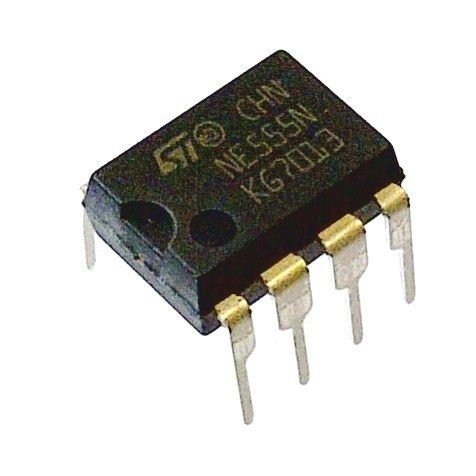
- It works from a wide range of power supplies ranging from +5V to +18V.
- Sourcing or sinking load current is 200mA.
- The external components must be selected correctly, so that the timing intervals can be completed in several minutes along with the frequencies beyond several hundred kHz.
- The o/p of a 555 timer IC can drive TTL due to its high current o/p.
- It takes a temperature stability of 50 ppm/oC change in temperature (ppm means parts per million)
- The timers duty cycle is adjustable.
- The max power dissipation per package is 600 milliwatts & its reset and trigger i/ps has logic compatibility.
-
-19%
 Out Of Stock
The AD7528 is a monolithic dual 8-bit digital/analog converter featuring excellent DAC-to-DAC matching. It is available in skinny 0.3″ wide 20-lead DIPs and in 20-lead surface mount packages. Separate on-chip latches are provided for each DAC to allow easy microprocessor interface.
-
-21%
 Out Of Stock
- HP2730 Opto Coupler IC
- Number of Channels: 2
- Voltage – Isolation: 2500 Vrms
- Current Transfer Ratio (Min): 300% @ 1.6 mA
- Turn On / Turn Off Time (Typ): 300 ns, 5 s
- Input Type: DC
- Output Type: Darlington
- Voltage – Output (Max): 7 V
- Current – Output / Channel: 60 mA
- Voltage – Forward (Vf) (Typ): 1.3 V
- Current – DC Forward (If) (Max): 20 mA
- Operating Temperature: -40C to 85C
- Mounting Type: Through Hole
- Package: 8-DIP (0.300″, 7.62mm)
-
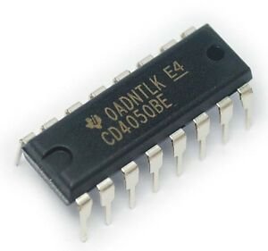
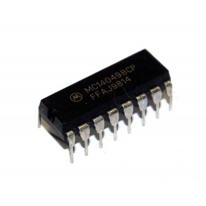
The CD4050 hex buffers are monolithic complementary MOS (CMOS) integrated circuits constructed with N- and P-channel enhancement mode transistors. These devices feature logic level conversion using only one supply voltage (VDD). The input signal high level (VIH) can exceed the VDD supply voltage when these devices are used for logic level conversions. These devices are intended for use as hex buffers, CMOS to DTL/ TTL converters, or as CMOS current drivers, and at VDD = 5.0V, they can drive directly two DTL/TTL loads over the full operating temperature range.
-

- Inverting IC that can convert High logic level to Low level
- High source and Sink Current as it has the capability of driving 2 TTL Loads at 5V over full temperature range.
- 100% Tested for Quiescent Current at 20 V
- Maximum Input Current of 1A at 18 V Over Full Package Temperature Range; 100 nA at 18 V and 25C
- 5-V, 10-V, and 15-V Parametric Ratings
- It is available in 16 pin packages of PDIP, SOIC, TSSOP, SO.
- Special input protection to protect inputs against static discharges.
-
- Wide supply voltage range: 3V to 15V
- Low power: 100 nW (typ.)
- High noise immunity: 0.45 VDD (typ.)
- Separate SET and RESET inputs for each latch
- NOR and NAND configuration
- 3-STATE output with common output enable
-
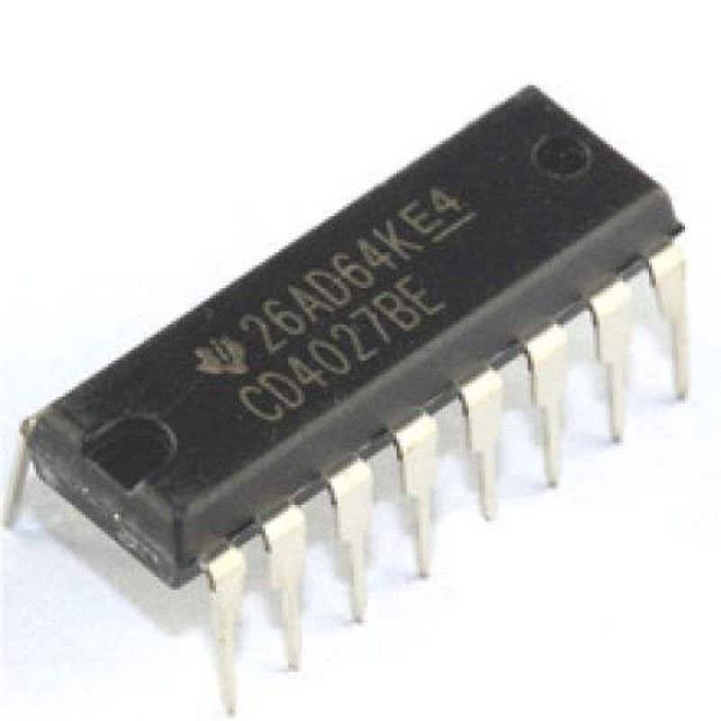
- CD4027 Dual JK Flip Flop Package IC which operates at medium speed of 16 MHz typically with 10V supply
- Voltage range of 3.0V to 15V
- Static Flip-Flop Operation
- High noise immunity of 0.45 VDD(typ.)
- Set and Reset capability
- TTL compatible
- Low power of 50 nW (typ.)
- Input Rise/Fall time at 5V: 45us
- Maximum and minimum Input Voltage is 2 V and 0.8 V
-
The CD4024 is a 7-stage ripple-carry binary counter. Buffered outputs are externally available from stages 1 through 7. The counter is reset to its logical 0 stage by a logical 1 on the reset input. The counter is advanced one count on the negative transition of each clock pulse.
-
-47%
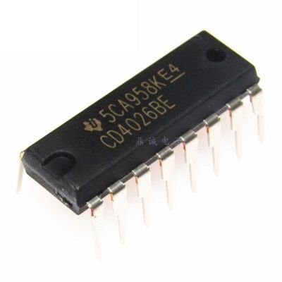
The IC CD4026 is an IC which can perform the function of both a counter as well a 7-segment Driver. One single IC can be used to count form zero (0) to nine (9) directly on a Common Cathode type 7-segment display. The count can be increased by simply giving a high clock pulse; also more than one digit (0-9) can be created by cascading more than one CD4026 IC. So if you have a 7-segment (CC) display on which you have to display numbers that are being counted based on some condition then this IC will be a perfect choice.
-
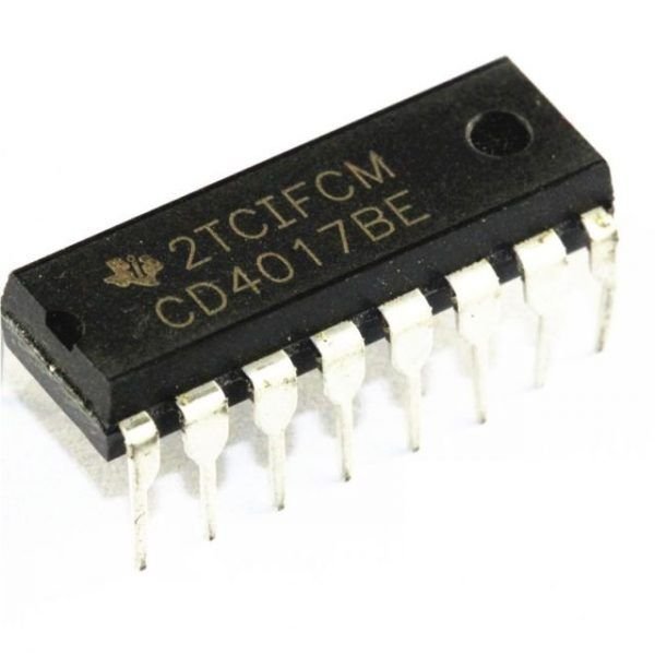
- The supply voltage of IC 4017 ranges from 3V to 15V, usually +5V
- This IC is well-matched with Transistor-Transistor Logic or TTL.
- The operational speed/CLK speed of this IC is 5 MHz.
- It provides support to10 outputs that are decoded.
- It is available in different packages like 16-pin GDIP, PDIP & PDSO
- Input high time 30 ns
- Output current is 10 mA
- Noise immunity is high typically 0.45 VDD
- Operation is completely static
- Low power like 10 W
- Speed operation is medium like 5.0 MHz with 10V VDD
- Input Voltage or Vin ranges from 0.5 VDC to VDD +0.5 VDC
- TS or Storage Temperature ranges from 65C to +150C
- VDD or DC Supply Voltage ranges from 0.5 VDC to +18 VDC
- PD or Power Dissipation is Dual-In-Line is 700 mW
- TL or Lead Temperature is 260C
-

- Asynchronous Set-Reset Capability
- Static Flip-Flop Operation
- Medium-Speed Operation: 16 MHz (Typical) Clock Toggle Rate at 10-V Supply
- Standardized Symmetrical Output Characteristics
- Maximum Input Current Of 1- A at 18 V Over Full Package Temperature Range:
- 100 nA at 18 V and 25C
- Noise Margin (Over Full Package Temperature Range):
- 1 V at VDD = 5 V
- 2 V at VDD = 10 V
- 2.5 V at VDD = 15 V
-

- Wide supply voltage range 3.0V to 15V
- Low power 10 nW (typ.)
- High noise immunity 0.45 VDD (typ.)
- Buffered Inputs and Outputs
- Standard Symmetrical Output Characteristics
- 100% Tested for Maximum Quiescent Current at 20V
- 5V, 10V and 15V Parametric Ratings
- Maximum Input Current of 1A at 18V Over Full Package-Temperature Range; 100nA at 18V and +25oC
-
- High Voltage Type (20V Rating)
- 3-State Parallel Outputs for Connection to Common Bus
- Separate Serial Outputs Synchronous to Both Positive and Negative Clock Edges for Cascading
- Medium Speed Operation – 5MHz at 10V (typ)
- Quiescent Current at 20V
- Maximum Input Current of 1A at 18V Over Full Package Temperature Range; 100nA at 18V and +25oC
- Noise Margin (Over Full Package/Temperature Range) – 1V at VDD = 5V – 2V at VDD = 10V – 2.5V at VDD = 15V
- 5V, 10V and 15V Parametric Ratings
-
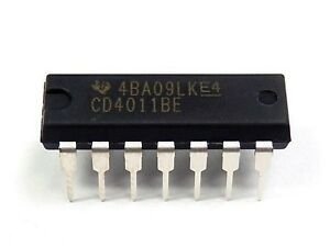
- Dual inputQuad NAND gate operation.
- Input voltage range: -0.5 to VDD +5V
- Power dissipation of 100mW per logic change.
- It is available in different outline packages
- The propagation delay time is 60ns
- All input and output pins are buffered for high throughput
- The output characteristics are standardized symmetric
- CD4011 draws a maximum input current of 1 Ampere at 18 volts
- Offers different noise margin level according to the input voltage level
- Temperature operating range is -55C to +125C
-
-30%

CD4051 Single 8-channel Multiplexer Demultiplexer
Original price was: ₨70.00.₨49.00Current price is: ₨49.00. Quick View- Analog and Digital Multiplexing and Demultiplexing
- A/D and D/A Conversion
- Signal Gating
- Factory Automation
- Televisions
- Appliances
- Consumer Audio
- Programmable Logic Circuits
- Sensors
-
The CD4081 quad gate is a monolithic complementary MOS (CMOS) integrated circuit constructed with N- and P-channel enhancement mode transistors. They have equal source and sink current capabilities and conform to standard B series output drive. The devices also have buffered outputs which improve transfer characteristics by providing very high gain. All inputs protected against static discharge with diodes to VDD and VSS.
-
- Operating Voltage: 5V, 10V, 15V DC
- Maximum Input Current: 1uA
- Hysteresis Voltage Typically 0.9 V at VDD: 5 V and 2.3 V at VDD: 10 V
- Noise Immunity Greater Than 50%
- Unlimited input rise and fall times
-
The 4077 is a quad 2-input EXCLUSIVE-NOR gate. The outputs are fully buffered for the highest noise immunity and pattern insensitivity to output impedance. The 4077 operates over a recommended VDD power supply range of 3 V to 15 V referenced to VSS (usually ground). Unused inputs must be connected to VDD, VSS, or another input.
-
- High Speed Binary Ripple Carry Counter
- Separate Reset Input Pin
- Wide Operating Voltage Range: 2.0 to 6.0 V
- Output Drive up to 10 LS-TTL Loads
- Equivalent to CD4060
-
- Dual Input IC with 4 OR Gates with an operating voltage range from 3V to 18V
- Fully Static and Medium Speed Operation: with tPHL, tPLH = 60ns (typ) at 10V
- DC input current: 10mA
- High-Voltage Type (20V Rating)
- Power Dissipation: 500mW
- Maximum propagation delay is 250ns.
- Standard symmetric output
- Minimum logic Low and High voltage @+5V is1.5V and 3.5V
- Maximum Transition Time is 200ns
-
- Wide range of digital and analog signal levels: digital 3 – 15V, analog to 15Vp-p
- Low “ON” resistance: 80Ω (typ.) over entire 15Vp-p
- signal-input range for VDD − VEE = 15V
- High “OFF” resistance:
- channel leakage of ±10 pA (typ.) at VDD − VEE = 10V
- Logic level conversion for digital addressing signals of
- 3 – 15V (VDD − VSS = 3 – 15V) to switch analog signals
- to 15 Vp-p (VDD − VEE = 15V)
- Binary address decoding on chip
-

- High-Voltage Types (20V Rating)
- CD4071BMS Quad 2-Input OR Gate
- CD4072BMS Dual 4-Input OR Gate
- CD4075BMS Triple 3-Input OR Gate
- Medium Speed Operation: tPHL, tPLH = 60ns (typ) at 10V
- 100% Tested for Quiescent Current at 20V
- Maximum Input Current of 1A at 18V Over Full Package Temperature Range; 100nA at 18V and +25oC
- Standardized Symmetrical Output Characteristics
-

- High-Voltage Types (20V Rating)
- CD4073BMS Triple 3-Input AND Gate
- CD4081BMS Quad 2-Input AND Gate
- CD4082BMS Dual 4-Input AND Gate
- Medium Speed Operation: tPLH, tPHL = 60ns (typ) at VDD = 10V
- 100% Tested for Quiescent Current at 20V
- Maximum Input Current of 1A at 18V Over Full Package Temperature Range; 100nA at 18V and +25oC
-
-34%

CD4538 – Dual Monostable Multivibrator
Original price was: ₨150.00.₨99.00Current price is: ₨99.00. Quick View- Wide supply voltage range 3.0V to 15V
- High noise immunity 0.45 VCC (typ.)
- Low power Fan out of 2 driving 74L TTL compatibility or 1 driving 74LS
- New formula: PWOUT e RC (PW in seconds, R in Ohms, C in Farads)
- g1.0% pulse-width variation from part to part (typ.) Wide pulse-width range 1 ms to %
- Separate latched reset inputs
- Symmetrical output sink and source capability
- Low standby current 5 nA (typ.) @ 5 VDC Y Pin compatible to CD4528
-

- Input levels: CMOS level
- 16-line demultiplexing capability
- Decodes 4 binary-coded inputs into 16 mutually-exclusive outputs
- Complies with JEDEC standard no. 7 A
- ESD protection: HBM JESD22-A114F exceeds 2000 V MM JESD22-A115-A exceeds 200V
- Multiple package options
- Specified from -40C to +85C and -40C to +125C
-
- Supply voltage ranges from 3v to 18v
- Set-up-time is 150, 70, and 40ns at 5v, 10v, and 15v respectively
- Strobe pulse width is 400, 160, and 100ns at 5v, 10v, and 15v respectively
- Hold time is zero
- 100% tested for quiescent current at 20v
- Having high input current of 1uA (max.) at 18v
- Maximum output current sourcing of 25mA
- Operating temperature ranges from -40 C to 85 C
- Storage temperature ranges from -65 C to 150 C
-
-40%
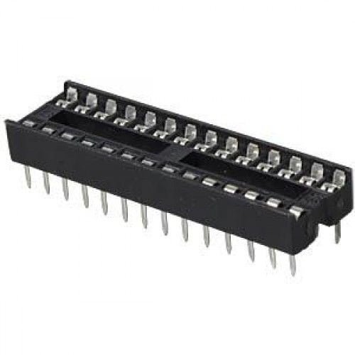
IC sockets are generally for preventing damage to IC’s from soldering and while testing multiple circuits. These are made from Black Thermoplastic and tin-plated alloy contacts. One end is notched to aid in identification. They can be mounted end to end to suit longer IC’s.
-
-17%

- Overall height above PCB: 4.8mm
- PCB hole required: 0.6mm
- Pitch Width: 7.62mm (0.3in)
- Pin Pitch: 2.54mm (0.1in)
- Pins: 16 pins
-
-18%
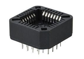
This is a IC Socket/Base for 28 pin SMD PLCC IC. This is a SMT base and is advisable on boards with point to point wiring because replacing a defective IC is time consuming and can possibly damage your prototype board. The use of an IC socket is inexpensive compared to the time and effort required to replace an IC chip. IC sockets also reduce the possibility of damaging the board when swapping out IC’s.
-
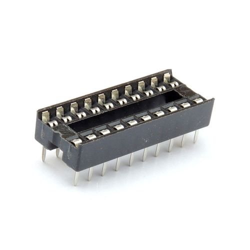
IC sockets are generally for preventing damage to IC’s from soldering and while testing multiple circuits. These are made from Black Thermoplastic and tin-plated alloy contacts. One end is notched to aid in identification. They can be mounted end to end to suit longer IC’s.
-
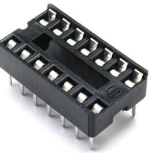
14 Pin – DIP IC Socket/Base IC sockets are generally for preventing damage to IC’s from soldering and while testing multiple circuits. These are made from Black Thermoplastic and tin-plated alloy contacts. One end is notched to aid in identification. They can be mounted end to end to suit longer IC’s.
-

-
Overall height above PCB: 4.8mm
-
PCB hole required: 0.6mm
-
Pitch Width: 7.62mm (0.3in)
- Pin Pitch: 2.54mm (0.1in)
- Pins: 14 pins
-
-

IC sockets are generally for preventing damage to IC’s from soldering and while testing multiple circuits. These are made from Black Thermoplastic and tin-plated alloy contacts. One end is notched to aid in identification. They can be mounted end to end to suit longer IC’s.
-
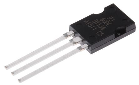
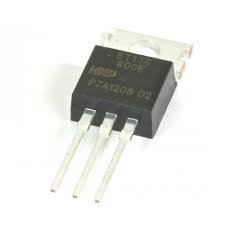
BT134 Triac – 600V – 4A (BT134-600E) Triac they are used in AC switching and control applications with current ratings from under 1A to 40A rms. Since TRIACs are bi-directional switching devices they are commonly used for switching AC applications. It has Maximum Terminal current: 4A, Max Terminal Voltage is 600 V, Gate trigger current: 25mA & On-state Gate voltage: 1.7V.
-
-36%

The HT12E Encoder ICs are series of CMOS LSIs for Remote Control system applications. They are capable of Encoding 12 bit of information which consists of 8 address bits and 4 data bits. Each address and data input is externally programmable or fed in using switches. The HT12D Decoder ICs are series of CMOS LSIs for Remote Control system applications. These ICs are paired with each other. For proper operation a pair of encoder/decoder with the same number of address and data format should be selected (HT12E is paired with HT12D). The Decoder receive the serial address and data, transmitted by a carrier using an RF transmission medium and gives output to the output pins after processing the data. These Ics have operating Voltage : 2.4V ~ 12V. They have Low Power and High Noise Immunity.
-
-14%
L293D IC Dual H-Bridge Motor Driver
Original price was: ₨150.00.₨129.00Current price is: ₨129.00. Quick View- It can be used to run Two DC motors with the same IC.
- Speed and Direction control is possible
- Motor driver voltage Vcc2 (Vs): 4.5V to 36V
- Maximum Peak motor current: 1.2A
- Maximum Continuous Motor Current: 600mA
- Supply Voltage to Vcc1(VSS): 4.5V to 7V
- Transition time: 300ns (at 5Vand 24V)
- Automatic Thermal shutdown is available
- Available in 16-pin DIP, TSSOP, SOIC packages
-
-18%
- HEX Inverter
- Logic Gate IC
- Not Gate | Inverter
- 7404
- SN74HC04N same as SN74LS04N
- IC 04 IC04
-
-18%
A flip flop is a device that is able to store single bit of data. It is either one or zero, off or on in this case. It is able to store data over a prolonged period of time. There are many applications of 74HC374 Flip Flop IC.
-
-18%
- Identical in Function to the 74LS93 with Different Pin Arrangement
- Contains Four Master-Slave Flips-Flops together with a Binary Counter
- Gated Zero Reset
- Fast Propagation Speeds
- Low Power Dissipation
-
-15%
This device contains four independent gates each of which performs the logic exclusive-OR function.
-
-16%
- Logic Type: INVERTER / NOR / NAND
- Output Current: 6.8mA
- Supply voltage range: 3V to 18V
- Package Type: DIP
- Pin number: 14
- Operating temperature range: -55 ° C to +125 ° C
- Surface Mount Devices: through-hole mounting
-
-41%
- Technology Family: LS
- Rating: Catalog
- Supply voltage: 1.0V to 5.5V
- Frequency at nominal voltage: 35 MHz
- Typical propagation delay: 21nS
- Low power consumption: 32mW
- Operating temperature: -40ºC to +125ºC
- ESD protection
- Balanced propagation delays
- Designed specifically for high speed
- Channels (#): 1
- Configuration: 3:8
- Product type: Standard
-
-33%
- Technology Family: CD4000
- VCC (Min) (V): 3
- VCC (Max) (V): 18
- Channels (#): 4
- Inputs per channel: 2
- IOL (Max) (mA): 6.8
- IOH (Max) (mA): -6.8
- Input type Standard: CMOS
- Output type: Push-Pull
- 5V–10V–15V parametric ratings
- Symmetrical output characteristics
- Speed: (tpd > 50ns)
- Data rate (Max) (Mbps): 8
- Rating: Catalog
- Operating temperature range (C): -55 to 125
-
-11%
SN74125 Buffer & Line Driver IC
Original price was: ₨55.00.₨49.00Current price is: ₨49.00. Quick View- Technology Family: LS
- VCC (Min): 4.75V
- VCC (Max): 5.25
- Channels (#): 4
- Operating Voltage (Nom): 5V
- Frequency at normal voltage (Max): 35MHz
- Propagation delay (Max): 20ns
- IOL (Max): 24mA
- IOH (Max):-2.6mA
- Input Type: Bi-polar
- Output type: 3-State
- High speed (tpd 10-50ns)
- Rating: Catalog
- Data rate: 70Mbps
- Available in 14-pin PDIP, GDIP, PDSO packages
-
-28%
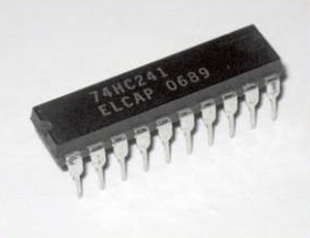
SN74HC241 Buffer & Line Driver IC
Original price was: ₨250.00.₨180.00Current price is: ₨180.00. Quick ViewThese octal buffers and line drivers are designed specifically to improve both the performance and density of 3-state memory address drivers, clock drivers, and bus-oriented receivers and transmitters. The HC241 devices are organized as two 4-bit buffers/drivers with separate output-enable (1OE and 2OE) inputs. When 1OE is low or 2OE is high, the device passes noninverted data from the A inputs to the Y outputs. When 1OE is high or 2OE is low, the outputs for the respective buffers/drivers are in the high-impedance state.
-
-22%
 Out Of Stock
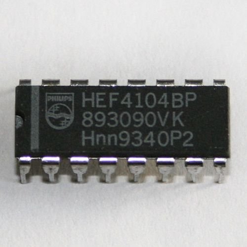
The HEF4104B is a quad low voltage-to-high voltage translator with 3-state outputs. It provides the capability of interfacing low voltage circuits to high voltage circuits. For example low voltage Local Oxidation Complementary MOS (LOCMOS) and Transistor-Transistor Logic (TTL) to high voltage LOCMOS. It has four data inputs (A0 to A3), an active HIGH output enable input (OE), four data outputs (B0 to B3) and their complements (B0 to B3).
-
- Maximum Terminal current: 4A
- On-state Gate voltage: 1.4V
- Gate trigger current: 10mA
- Max Terminal Voltage is 600 V
- Holding current: 2.2mA
- Latching current: 4mA
- Available in To-220 Package
-
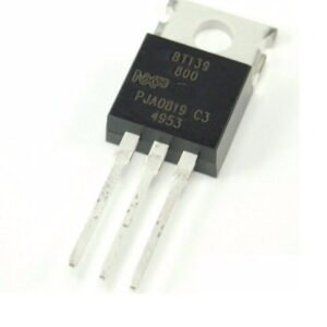
The BT139 is a TRIAC thyristor, which is a type of semiconductor device that can use to control alternating current (AC) power. TRIAC thyristor BT139 is a four-quadrant device, meaning that it can conduct current in either direction. The BT139 has a peak inverse voltage (PIV) of 800 volts and a current rating of 16 amperes. It is a sensitive gate triac, meaning that it can be triggered with a low gate current. The on-state voltage drop of the BT139 is 1.2 volts. Here are some of the key features of the BT139-800E 4 Quadrant TRIAC:
- Peak inverse voltage (PIV): 800 V
- RMS current: 16 A
- Gate trigger current: 2.5 mA
- Gate trigger voltage: 1.4 V
- On-state voltage drop: 1.2 V
- Thermal resistance: 1.2 K/W (junction to mounting base)
- Operating temperature range: -40 to 125 °C
-
-25%
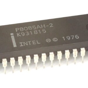
The 8085 is an 8-bit general purpose microprocessor that can address 64K Byte of memory. It has 40 pins and uses +5V for power. It can run at a maximum frequency of 3 MHz.
-
-33%
- Output current (single output): 500 mA (max)
- High sustaining voltage output: 50 V (min)
- Output clamp diodes
- Inputs compatible with various types of logic.
- Package type-AFG: SOP-18 pin
-

The MC34063A Series is a monolithic control circuit containing the primary functions required for dc-to-dc converters. These Buck Boost Inverting Switching Regulators consist of an internal temperature compensated reference, comparator, controlled duty cycle oscillator with an active current limit circuit, driver and high current output switch. Operation from 3.0 V to 40 V Input. Output Switch Current to 1.5 A.
-
-13%

- Ultra Low Power Consumption 0.7 μA
- Wide Range of Supply Voltages 2V to 8V
- Input Common-Mode Range Beyond V+ and V−
- Open Collector and Push-Pull Output
- High Output Current Drive: (@ VS = 5V) 45 mA
- Propagation Delay (@ VS = 5V, 10 mV Overdrive) 25 μs
- Tiny 5-Pin SOT-23 Package
- Latch-up Resistance >300 mA
- LMC7215-Q1 is an Automotive Grade Product that is AEC-Q100 Grade 3 Qualified.
-
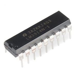
-26%
- Analog Controlled LED Driver IC with Logarithmic output
- LED incremented by one step for every 3dB
- Monitor upto 30dB using 10 LEDs
- Number of controllable LEDs: 10
- Operating Voltage: 3V to 25V
- Reference Voltage: 1.2V to 12V
- LED sink current: 1mA to 30mA (programmable)
- Both Dot/Bar mode available
- Available in 18-pin DIP, PLCC package
-
-54%
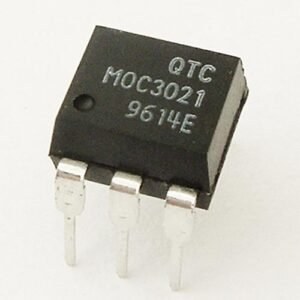
MOC3021 Triac Driven Optoisolator
Original price was: ₨150.00.₨69.00Current price is: ₨69.00. Quick View- Opto-isolator with Zero-Crossing Triac Driver
- Input LED Diode Forward Voltage: 1.15V
- LED Forward Latch Current: 15mA
- TRIAC output terminal voltage: 400V (max)
- TRIAC peak output current: 1A
- Available as 6-pin PDIP with and without M-suffix
-
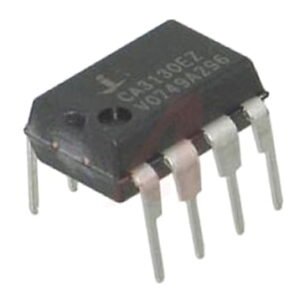
- Op-amp coupled with MOSFET at output
- Wide power supply Range
- Singe supply – 5V to 16V
- Dual supply – ±2.5V to ±8V
- Input Terminal current: 1mA
- Maximum Output Voltage: 13.3V
- Maximum source current: 22mA
- Maximum sink current: 20mA
- Supply current: 10mA
- Common Mode Rejection Ration (CMRR): 80dB
-
-46%
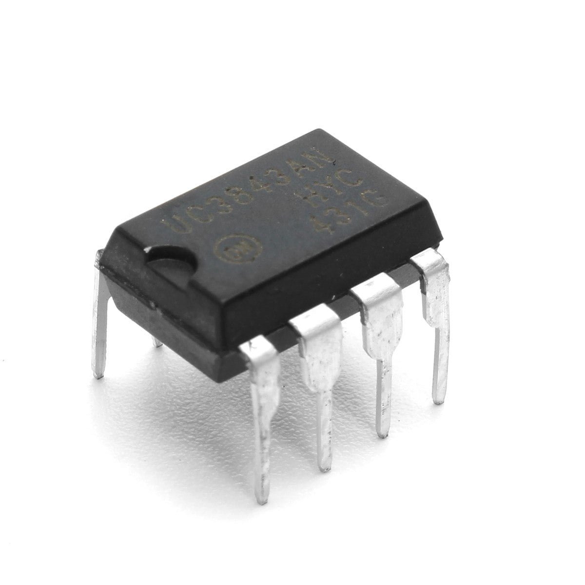
- Current-Mode PWM controller
- Operating Voltage: 7.0V to 8.2V
- Output pin current: 1A
- Analog input range: -0.3 to 6.3V
- Oscillation Frequency: 52 Typically
- Gain: 3V
- Maximum source current: 22mA
- Low Output Voltage: 0.08V
- High Output Voltage: 13.5V
-
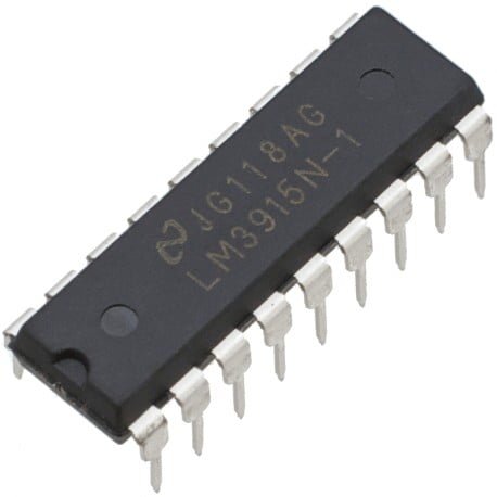
-20%
- Analog Controlled LED Driver IC
- Number of controllable LEDs: 10
- Operating Voltage: 3V to 18V
- Input Analog voltage range: 1.2V to 12V
- LED sink current: 2mA to 30mA (programmable)
- Both Dot/Bar mode available
- Can be cascaded to control upto 100 LEDs
- Available in 18-pin DIP package