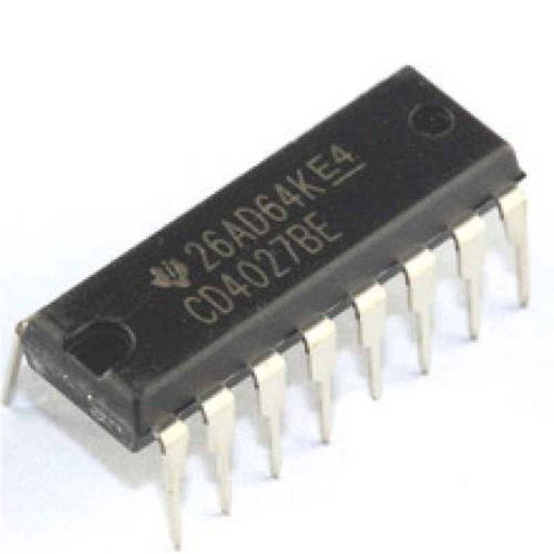
CD4027 – Dual JK FlipFlop
CD4027 – Dual JK FlipFlop, When we want to use flip-flops with CMOS. Often we meet CD4027. It is dual J-K flip-flops that are monolithic complementary MOS integrated circuits.
We have seen many circuits that use them. Of course, making a great circuit we should understand detail of any parts( basic enough).
Slow down!
If you are beginner. You should read how flip-flop works below.
Pin Configuration Description
This CD4027 IC has a total of 16 pins. As it is a dual flip flop IC, so it has 2 flip flops. All the pins, their name, and description are mentioned in the table given below.
| Pin Number | Pin Name | Description |
|---|---|---|
| 1, 15 | Q2, Q1 | Output pins |
| 2, 14 | , | Inverted Output pins |
| 3, 13 | CLOCK 2, CLOCK 1 | Clock pulse |
| 4, 12 | RESET 2, RESET 1 | When this pin is LOW, the value of Q will be 1.
When this pin is HIGH, the value of inverted output () will be 1. |
| 5, 11 | K2, K1 | Input Pin 1 |
| 6, 10 | J2, J1 | Input pin 2 |
| 7, 9 | SET 2, SET 1 | When this pin is HIGH, the value of Q will be 1.
When this pin is LOW, the value of inverted output () will be high. |
| 8 | Negative power Supply | |
| 16 | Positive power supply |
CD4027 Features
- CD4027 Dual JK Flip Flop Package IC which operates at medium speed of 16 MHz typically with 10V supply
- Voltage range of 3.0V to 15V
- Static Flip-Flop Operation
- High noise immunity of 0.45 VDD(typ.)
- Set and Reset capability
- TTL compatible
- Low power of 50 nW (typ.)
- Input Rise/Fall time at 5V: 45us
- Maximum and minimum Input Voltage is 2 V and 0.8 V
Where to use it
This CD4027IC is used for storing data and in performing control, register, and toggle functions. In toggling applications, it is used to alter the signal by control inputs. You can also use this IC in latching devices due to its property of storing data and determining the output based on the previous output.
How to use CD4027
CD4027 has two flip flops each having independent four inputs and two outputs that work opposite to each other. The input pins J and K control the state of flip flop which occurs at the positive transition of clock pulse. We can provide a clock signal through a push button or a PWM signal. Set and reset pins are independent of the clock. They are initiated by applying a High signal on these pins. Pin 8 is connected to the ground. Connect pin 16 with power supply and switch on the supply.


Reviews
There are no reviews yet.