CD4011 – Quad 2-Input NAND Gate
CD4011 – Quad 2-Input NAND Gate IC. It is a quadrable NAND gate integrated circuit that means it consists of 4 NAND gatesin a single unit. It is based on CMOS logic. All inputs and outputs are designed according to the CMOS logic voltage level. It is used to execute NAND logic or you can use a combination of four gates to perform AND A= X x Y or OR B = X+Y operation also. All logical inputs and outputs of NAND. I/O pins are buffered for throughput.
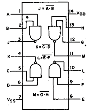
Pin configuration details CD4011
This table provides details of all pins given in the above pinout.
| Pin number | Pin Name | Function |
|---|---|---|
| 1 | INPUT A | Input pin first NAND gate |
| 2 | INPUT B | Input pin first NAND gate |
| 3 | OUTPUT J | Output pin first NAND gate |
| 4 | OUTPUT K | Output pin 2nd NAND gate |
| 5 | INPUT C | Input pin 2nd NAND gate |
| 6 | INPUT D | Input pin 2nd NAND gate |
| 7 | GND | Connect with ground pin |
| 8 | INPUT E | Input pin 3rd NAND gate |
| 9 | INPUT F | Input pin 3rd NAND gate |
| 10 | OUTPUT L | Output pin 3rd NAND gate |
| 11 | OUTPUT M | Output pin 4th NAND gate |
| 12 | INPUT G | Input pin 4th NAND gate |
| 13 | INPUT H | Input pin 4th NAND gate |
| 14 | VCC/VDD | Connect with 5 volts power supply |
Features of CD4011
- Dual inputQuad NAND gate operation.
- Input voltage range: -0.5 to VDD +5V
- Power dissipation of 100mW per logic change.
- It is available in different outline packages
- The propagation delay time is 60ns
- All input and output pins are buffered for high throughput
- The output characteristics are standardized symmetric
- CD4011 draws a maximum input current of 1 Ampere at 18 volts
- Offers different noise margin level according to the input voltage level
- Temperature operating range is -55C to +125C
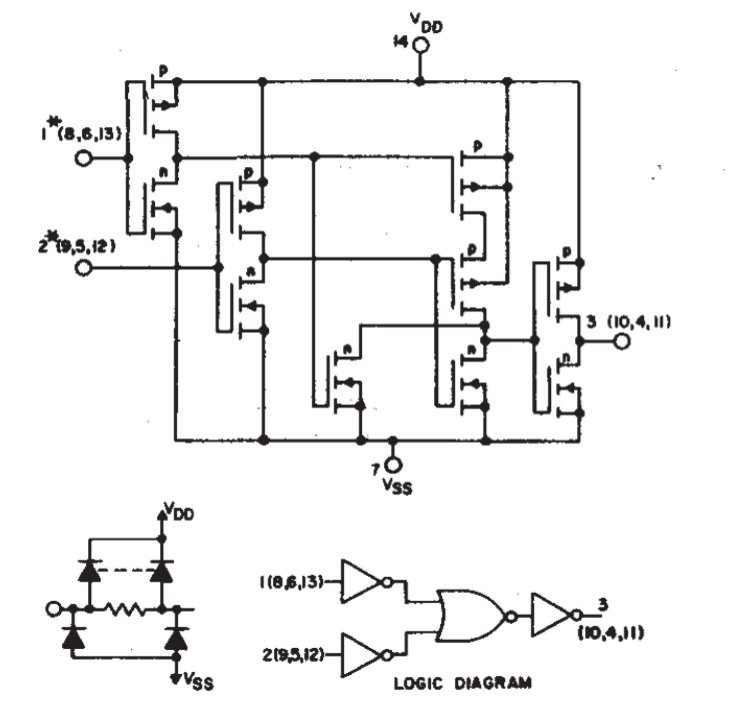
Internal Structure of CD4011
If you see a transistor level logic diagram, CD4011 consists of NMOS and PMOS transistors and logic for this high operation NAND gate is based on NOT and NOR gates.
Where to use CD4011
As mentioned earlier, CD4011 is an 8-bit CMOS based quad NAND gate IC. It consists of 4 NAND gates which can be used to implement the logic of other gates such as NOT, AND and OR. It can also be used in applications wherehigh-speed NAND outputis required as this chip can provide output in less than 60ns. To make high-speed operation, we always need a circuit with low transition time. In short, it is the recommended logic gate for high-frequency systems.
How to use NAND gate IC
As we have already discussed in detail about the pinout and pin configuration ofCD4011 8-bit NAND IC, it has four NAND gates. To understand its working, let’s first understand how NAND gate works. The table shown here demonstrates the logical function of the NAND gate.
| INPUT A | INPUT B | OUTPUT |
|---|---|---|
| LOW (0) | LOW (0) | HIGH (1) |
| LOW (0) | HIGH (1) | HIGH (1) |
| HIGH (1) | LOW (0) | HIGH (1) |
| HIGH (1) | HIGH (1) | LOW (0) |
As you can see from the above table, the output of the logic gate is low only when both inputs are logical high. It has 12 I/O pins out of which 4 pins are output pins and 8 are inputs pins. The internal circuit diagram depicts the I/O pins clearly.
Application of CD4011 8-bit NAND gate IC
- Decoders
- Multiplexers
- Logic gates
- Audio players
- AV based receivers and transmitters
- Digital locks
- safety thermostats
DOWNLOAD DATASHEET


Reviews
There are no reviews yet.