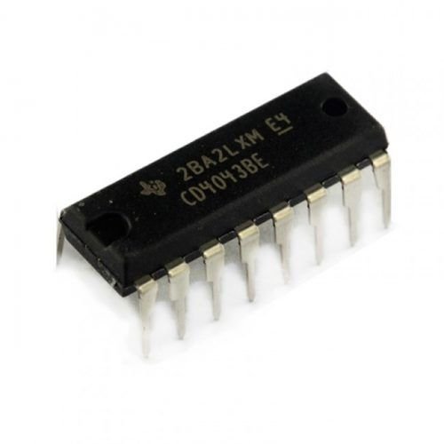
CD4043 Quad NOR R-S Latch Tri-state
CD4043 Quad NOR R-S Latch Tri-state is a combinational logic circuit, that has two inputs S and R, and two outputs Q and Q. The state of this latch is determined by the condition of output Q. If output Q is 1 (High) the latch is said to be SET and if Q is 0 (Low) the latch is said to be RESET. An SR Latch or Flip flop can be designed either by two cross-coupled NAND gates or two-cross coupled NOR gates.
CD4043 Key Features
- Wide supply voltage range: 3V to 15V
- Low power: 100 nW (typ.)
- High noise immunity: 0.45 VDD (typ.)
- Separate SET and RESET inputs for each latch
- NOR and NAND configuration
- 3-STATE output with common output enable
CD4043 Pinout
| Pin No | Pin Name | Description |
|---|---|---|
| 1 | Q4 | output of latch 4 |
| 2 | Q1 | output of latch 1 |
| 3 | R1 | reset input latch 1 |
| 4 | S1 | set input latch 1 |
| 5 | ENB | enable pin |
| 6 | S2 | set input latch 2 |
| 7 | R2 | reset input latch 2 |
| 8 | VSS | source supply |
| 9 | Q2 | output of latch 2 |
| 10 | Q3 | output of latch 3 |
| 11 | R3 | reset input latch 3 |
| 12 | S3 | set input latch 3 |
| 13 | NC | no connection |
| 14 | S4 | set input latch 4 |
| 15 | R4 | reset input latch 4 |
| 16 | VDD | Drain supply |
Application
- Multiple bus storage
- Strobed register
- Four bits of independent storage with output enable
- General digital logic
CD4043 Datasheet
You can download the datasheet for CD4043 Quad NOR R-S Latch with Tristate


Reviews
There are no reviews yet.