-

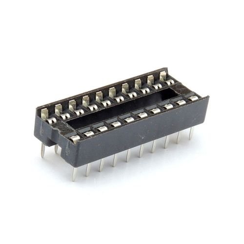
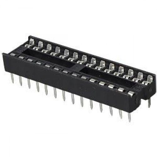
IC sockets are generally for preventing damage to IC’s from soldering and while testing multiple circuits. These are made from Black Thermoplastic and tin-plated alloy contacts. One end is notched to aid in identification. They can be mounted end to end to suit longer IC’s.
-
-40%
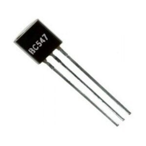

BC547-B166 NPN Transistor 50V/ 0.3A
Original price was: ₨15.00.₨9.00Current price is: ₨9.00. Quick ViewOverall, the BC547 NPN transistor is a versatile and reliable transistor that is suitable for a wide range of applications. NPN Transistor BC547 is a popular choice for electronic hobbyists and engineers because it is inexpensive and easy to use. here are the specifications of the BC547-B166 NPN transistor:
- Collector current (maximum): 300mA
- Collector-emitter voltage (maximum): 65V
- Base current (maximum): 5mA
- Current gain (hFE): 110 to 800
- Package: TO-92
-

-
Overall height above PCB: 4.8mm
-
PCB hole required: 0.6mm
-
Pitch Width: 7.62mm (0.3in)
- Pin Pitch: 2.54mm (0.1in)
- Pins: 14 pins
-
-
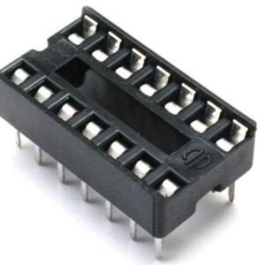
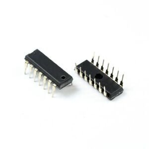
14 Pin – DIP IC Socket/Base IC sockets are generally for preventing damage to IC’s from soldering and while testing multiple circuits. These are made from Black Thermoplastic and tin-plated alloy contacts. One end is notched to aid in identification. They can be mounted end to end to suit longer IC’s.
-
-17%

- Overall height above PCB: 4.8mm
- PCB hole required: 0.6mm
- Pitch Width: 7.62mm (0.3in)
- Pin Pitch: 2.54mm (0.1in)
- Pins: 16 pins
-
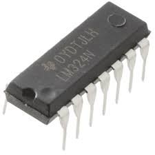
LM324 Operational Amplifier IC LM-324 consist of four independent high-gain frequency-compensated operational amplifiers that are designed specifically to operate from a single supply or split supply over a wide range of voltages. Wide Supply Ranges Single Supply: 3 V to 32 V (26 V for LM2902) Dual Supplies: 1.5 V to 16 V (13 V for LM2902) Low Supply-Current Drain.
-
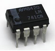
The LM741 series are general-purpose operational amplifiers which feature improved performance over industry.The amplifiers offer many features : overload protection on the input and output, no latch-up when the common-mode range is exceeded, as well as freedom from oscillations. The LM741C is identical to the LM741 and LM741A except that the LM741C has their performance ensured over a 0C to +70C temperature range, instead of 55C to +125C.
-
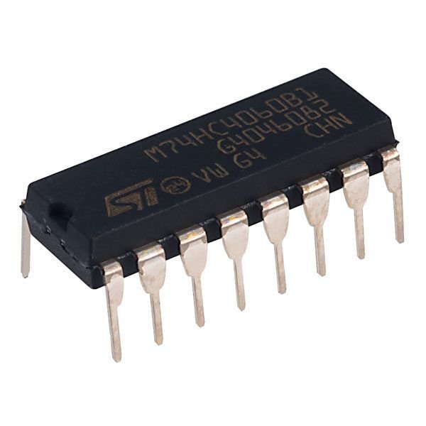
- Low Voltage and Standard-Voltage Operation
- 2-wire Serial Interface
- Schmitt Trigger, Filtered Inputs for Noise Suppression
- Bi-directional Data Transfer Protocol
- 100kHz and 400kHz Compatibility
- Write Protect Pin for Hardware Data Protection
- 8-byte Page (1K, 2K), 16-byte Page (4K, 8K, 16K) Write Modes
- Partial Page Writes are Allowed
- Self-timed Write Cycle (10mS max)
-
BT134 Triac – 600V – 4A (BT134-600E) Triac they are used in AC switching and control applications with current ratings from under 1A to 40A rms. Since TRIACs are bi-directional switching devices they are commonly used for switching AC applications. It has Maximum Terminal current: 4A, Max Terminal Voltage is 600 V, Gate trigger current: 25mA & On-state Gate voltage: 1.7V.
-

The SN74HC244N is an Octal Buffer and Line Driver IC, designed specifically to improve both the performance and density of 3-state memory address drivers, clock drivers and bus-oriented receivers and transmitters. This device organized as two 4-bit buffers/drivers with separate output-enable (OE)/inputs. When OE/ is low, the device passes non-inverted data from the A inputs to the Y outputs. When OE/ is high, the outputs are in the high-impedance state.
-

The 4072 is a member of the 4000 Series CMOS range, and contains two independent OR gates, each with four inputs.
-

The CD4040 is a 12-stage ripple carry binary counter. The counters are advanced one count on the negative transition of each clock pulse. The counters are reset to the zero state by a logical 1 at the reset input independent of the clock.
-
The voltage regulator IC maintains the output voltage at a constant value. 7805 provides +5V regulated power supply. Input voltage range 7V- 35V Current rating Ic = 1A Output voltage range VMax=5.2V ,VMin=4.8V.
-
-38%
- It works from a wide range of power supplies ranging from +5V to +18V.
- Sourcing or sinking load current is 200mA.
- The external components must be selected correctly, so that the timing intervals can be completed in several minutes along with the frequencies beyond several hundred kHz.
- The o/p of a 555 timer IC can drive TTL due to its high current o/p.
- It takes a temperature stability of 50 ppm/oC change in temperature (ppm means parts per million)
- The timers duty cycle is adjustable.
- The max power dissipation per package is 600 milliwatts & its reset and trigger i/ps has logic compatibility.
-
Texas Instruments SN7414 Series Inverters are available at ElectroNation.
-
- Carries Low input bias current = 50 pA
- Available with Low input noise current = 0.01 pA/Hz
- Comes with Fast settling time to 0.01% = 2us
- Contains internally trimmed offset voltage = 15 mV
- Carries Low input noise voltage = 16nV/Hz
- Exhibits Low supply current = 3.6 mA
-
-17%
LM386 LM-386 Audio Amplifier Chip
Original price was: ₨35.00.₨29.00Current price is: ₨29.00. Quick ViewLM386 is a widely used audio amplifier IC manufactured in 8 pin dip, VSSOP, SOIC and other packages. The IC is basically designed for low voltage commercial applications, apart from commercial applications it is also a famous IC among electronic hobbyists and experimenters. The internal gain of the IC is set to 20 but it can be adjusted by connecting a resistor and a capacitor in series between the pin number 1 and 8, by this procedure the user can adjust the gain between 20 to 200. Due to the small size, low quiescent current and low voltage requirements this IC is ideal to use in wide variety of portable battery operated applications and devices.
-
-36%
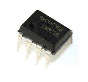
LM393 Dual COMPARATOR Low Offset Voltage IC
Original price was: ₨45.00.₨29.00Current price is: ₨29.00. Quick View- Voltage Comparator circuits
- Can drive Relay, Lamp, Motor Etc
- Zero Crossing detector
- Peak voltage Detector
- High Voltage protection/Warning
- Oscillator circuits
-
-36%
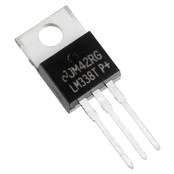
LM338T 5A Adjustable Voltage Regulator LM-338T
Original price was: ₨45.00.₨29.00Current price is: ₨29.00. Quick ViewLM338T 5A Adjustable Voltage Regulator LM-338T is adjustable 3-terminal positive voltage regulators is capable of supplying in excess of 5 A over a 1.2-V to 32-V output range. They are exceptionally easy to use and require only 2 resistors to set the output voltage.
-
-36%

LM358 LM358P DIP8 LM 358 LM358N DIP-8 IC
Original price was: ₨45.00.₨29.00Current price is: ₨29.00. Quick View- Very low supply current drain (500 A) essentially independent of supply voltage
- Low input offset voltage: 2 mV
- Input common-mode voltage range includes ground
- Differential input voltage range equal to the power supply voltage
- Large output voltage swing: 0V to V+ 1.5V
- Internally frequency compensated for unity gain
- Large dc voltage gain: 100 dB
- Wide bandwidth (unity gain): 1 MHz (temperature compensated)
-
IC sockets are generally for preventing damage to IC’s from soldering and while testing multiple circuits. These are made from Black Thermoplastic and tin-plated alloy contacts. One end is notched to aid in identification. They can be mounted end to end to suit longer IC’s.
-

- Microcontrollers I/O switching
- VoIP phones
- Signal isolation
- PC communications
-
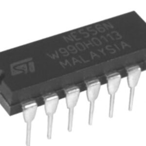
- A dual version of NE556 consists of two precision timers that operate in both monostable and astable modes.
- It is specified for operation from 4.5 V to 16 V.
- TTL compatible output which can source or sink current of up to 150mA.
- Adjustable duty cycle.
- It can produce a timing delay from microseconds to hours.
- The operating temperature range is from 0 to 70 degrees Celsius.
- It has temperature stability better than 0.005% per C.
-
- Low-voltage and Standard-voltage Operation
- 2.7 (VCC = 2.7V to 5.5V)
- 1.8 (VCC = 1.8V to 5.5V)
- Internally Organized 128 x 8 (1K), 256 x 8 (2K), 512 x 8 (4K),
- 1024 x 8 (8K) or 2048 x 8 (16K)
- Two-wire Serial Interface
- Schmitt Trigger, Filtered Inputs for Noise Suppression
- Bidirectional Data Transfer Protocol
- 100 kHz (1.8V) and 400 kHz (2.7V, 5V) Compatibility
- Write Protect Pin for Hardware Data Protection
- 8-byte Page (1K, 2K), 16-byte Page (4K, 8K, 16K) Write Modes
- Partial Page Writes Allowed
- Self-timed Write Cycle (5 ms max)
- High-reliability
- Endurance: 1 Million Write Cycles
- Data Retention: 100 Years
- Automotive Devices Available
- 8-lead JEDEC PDIP, 8-lead JEDEC SOIC, 8-lead Ultra Thin Mini-MAP (MLP 2×3), 5-lead SOT23, 8-lead TSSOP and 8-ball dBGA2 Packages
- Die Sales: Wafer Form, Waffle Pack and Bumped Wafers
- Low-voltage and Standard-voltage Operation
-
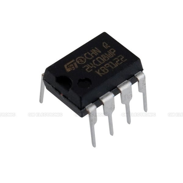 Out Of Stock
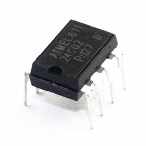
The M24C08 is an 8-Kbit I2C-compatible EEPROM (Electrically Erasable PROgrammable Memory) organized as 1 K 8 bits. It operate with a clock frequency of 400 kHz.
-
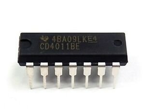
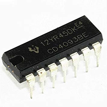
- Dual inputQuad NAND gate operation.
- Input voltage range: -0.5 to VDD +5V
- Power dissipation of 100mW per logic change.
- It is available in different outline packages
- The propagation delay time is 60ns
- All input and output pins are buffered for high throughput
- The output characteristics are standardized symmetric
- CD4011 draws a maximum input current of 1 Ampere at 18 volts
- Offers different noise margin level according to the input voltage level
- Temperature operating range is -55C to +125C
-

- Asynchronous Set-Reset Capability
- Static Flip-Flop Operation
- Medium-Speed Operation: 16 MHz (Typical) Clock Toggle Rate at 10-V Supply
- Standardized Symmetrical Output Characteristics
- Maximum Input Current Of 1- A at 18 V Over Full Package Temperature Range:
- 100 nA at 18 V and 25C
- Noise Margin (Over Full Package Temperature Range):
- 1 V at VDD = 5 V
- 2 V at VDD = 10 V
- 2.5 V at VDD = 15 V
-
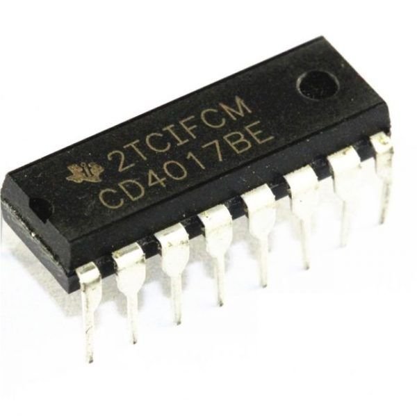
- The supply voltage of IC 4017 ranges from 3V to 15V, usually +5V
- This IC is well-matched with Transistor-Transistor Logic or TTL.
- The operational speed/CLK speed of this IC is 5 MHz.
- It provides support to10 outputs that are decoded.
- It is available in different packages like 16-pin GDIP, PDIP & PDSO
- Input high time 30 ns
- Output current is 10 mA
- Noise immunity is high typically 0.45 VDD
- Operation is completely static
- Low power like 10 W
- Speed operation is medium like 5.0 MHz with 10V VDD
- Input Voltage or Vin ranges from 0.5 VDC to VDD +0.5 VDC
- TS or Storage Temperature ranges from 65C to +150C
- VDD or DC Supply Voltage ranges from 0.5 VDC to +18 VDC
- PD or Power Dissipation is Dual-In-Line is 700 mW
- TL or Lead Temperature is 260C
-
The CD4024 is a 7-stage ripple-carry binary counter. Buffered outputs are externally available from stages 1 through 7. The counter is reset to its logical 0 stage by a logical 1 on the reset input. The counter is advanced one count on the negative transition of each clock pulse.
-
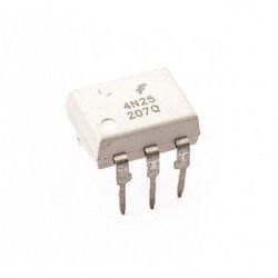
The 4N25 is an optocoupler for general purpose applications. It contains a light emitting diode optically coupled to a photo-transistor.
-
This is a monostable multivibrator or pulse generator.
-

The MC34063A Series is a monolithic control circuit containing the primary functions required for dc-to-dc converters. These Buck Boost Inverting Switching Regulators consist of an internal temperature compensated reference, comparator, controlled duty cycle oscillator with an active current limit circuit, driver and high current output switch. Operation from 3.0 V to 40 V Input. Output Switch Current to 1.5 A.
-
- High Speed Binary Ripple Carry Counter
- Separate Reset Input Pin
- Wide Operating Voltage Range: 2.0 to 6.0 V
- Output Drive up to 10 LS-TTL Loads
- Equivalent to CD4060
-
- Operating Voltage: 5V, 10V, 15V DC
- Maximum Input Current: 1uA
- Hysteresis Voltage Typically 0.9 V at VDD: 5 V and 2.3 V at VDD: 10 V
- Noise Immunity Greater Than 50%
- Unlimited input rise and fall times
-
- High Voltage Type (20V Rating)
- 3-State Parallel Outputs for Connection to Common Bus
- Separate Serial Outputs Synchronous to Both Positive and Negative Clock Edges for Cascading
- Medium Speed Operation – 5MHz at 10V (typ)
- Quiescent Current at 20V
- Maximum Input Current of 1A at 18V Over Full Package Temperature Range; 100nA at 18V and +25oC
- Noise Margin (Over Full Package/Temperature Range) – 1V at VDD = 5V – 2V at VDD = 10V – 2.5V at VDD = 15V
- 5V, 10V and 15V Parametric Ratings
-
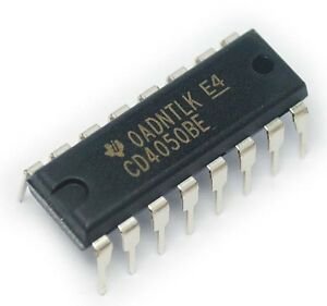
The CD4050 hex buffers are monolithic complementary MOS (CMOS) integrated circuits constructed with N- and P-channel enhancement mode transistors. These devices feature logic level conversion using only one supply voltage (VDD). The input signal high level (VIH) can exceed the VDD supply voltage when these devices are used for logic level conversions. These devices are intended for use as hex buffers, CMOS to DTL/ TTL converters, or as CMOS current drivers, and at VDD = 5.0V, they can drive directly two DTL/TTL loads over the full operating temperature range.
-
The 74LS139 is a high speed Dual 1-of-4 Decoder/De-multiplexer. The device has two independent decoders, each accepting two inputs and providing four mutually exclusive active LOW Outputs. Each decoder has an active LOW Enable input which can be used as a data input for a 4-output demultiplexer. Each half of the LS139 can be used as a function generator providing all four minterms of two variables. The LS139 is fabricated with the Schottky barrier diode process for high speed and is completely compatible with all Motorola TTL families.
-
- Operates from single 5V supply
- Input current: 150 nA max. over temperature
- Offset current: 20 nA max. over temperature
- Differential input voltage range: 30V
- Power consumption: 135 mW at 15V
- Available in Q-Temp Automotive
- High-Reliability Automotive Applications
- Configuration Control and Print Support
- Qualification to Automotive Standards
-
-13%

- Ultra Low Power Consumption 0.7 μA
- Wide Range of Supply Voltages 2V to 8V
- Input Common-Mode Range Beyond V+ and V−
- Open Collector and Push-Pull Output
- High Output Current Drive: (@ VS = 5V) 45 mA
- Propagation Delay (@ VS = 5V, 10 mV Overdrive) 25 μs
- Tiny 5-Pin SOT-23 Package
- Latch-up Resistance >300 mA
- LMC7215-Q1 is an Automotive Grade Product that is AEC-Q100 Grade 3 Qualified.
-
-33%

- Technology Family: CD4000
- VCC (Min) (V): 3
- VCC (Max) (V): 18
- Channels (#): 4
- Inputs per channel: 2
- IOL (Max) (mA): 6.8
- IOH (Max) (mA): -6.8
- Input type Standard: CMOS
- Output type: Push-Pull
- 5V–10V–15V parametric ratings
- Symmetrical output characteristics
- Speed: (tpd > 50ns)
- Data rate (Max) (Mbps): 8
- Rating: Catalog
- Operating temperature range (C): -55 to 125
-
-40%
IC sockets are generally for preventing damage to IC’s from soldering and while testing multiple circuits. These are made from Black Thermoplastic and tin-plated alloy contacts. One end is notched to aid in identification. They can be mounted end to end to suit longer IC’s.
-
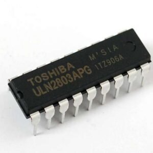
ULN 2803 is a high-voltage, high-current Darlington transistor array. The device consists of eight npn Darlington pairs that feature high-voltage outputs with common-cathode clamp diodes for switching inductive loads. The collector-current rating of each Darlington pair is 500 mA. The Darlington pairs may be connected in parallel for higher current capability. Applications include relay drivers, hammer drivers, lamp drivers, display drivers (LED and gas discharge), line drivers, and logic buffers.
-
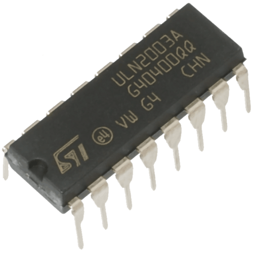
- Seven Darlingtons per package
- Output current 500 mA per driver (600 mA peak)
- Output voltage 50 V
- Integrated suppression diodes for inductive loads
- Outputs can be paralleled for higher current
- TTL/CMOS/PMOS/DTL compatible inputs
- Inputs pinned opposite outputs to simplify
-
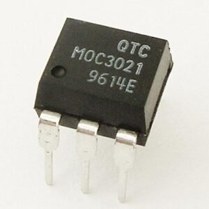
- Opto-isolator with Zero-Crossing Triac Driver
- Input LED Diode Forward Voltage: 1.15V
- LED Forward Latch Current: 15mA
- TRIAC output terminal voltage: 400V (max)
- TRIAC peak output current: 1A
- Available as 6-pin PDIP with and without M-suffix
-
- Dual Input IC with 4 OR Gates with an operating voltage range from 3V to 18V
- Fully Static and Medium Speed Operation: with tPHL, tPLH = 60ns (typ) at 10V
- DC input current: 10mA
- High-Voltage Type (20V Rating)
- Power Dissipation: 500mW
- Maximum propagation delay is 250ns.
- Standard symmetric output
- Minimum logic Low and High voltage @+5V is1.5V and 3.5V
- Maximum Transition Time is 200ns
-
The CD4081 quad gate is a monolithic complementary MOS (CMOS) integrated circuit constructed with N- and P-channel enhancement mode transistors. They have equal source and sink current capabilities and conform to standard B series output drive. The devices also have buffered outputs which improve transfer characteristics by providing very high gain. All inputs protected against static discharge with diodes to VDD and VSS.
-
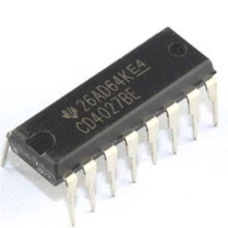
- CD4027 Dual JK Flip Flop Package IC which operates at medium speed of 16 MHz typically with 10V supply
- Voltage range of 3.0V to 15V
- Static Flip-Flop Operation
- High noise immunity of 0.45 VDD(typ.)
- Set and Reset capability
- TTL compatible
- Low power of 50 nW (typ.)
- Input Rise/Fall time at 5V: 45us
- Maximum and minimum Input Voltage is 2 V and 0.8 V
-

- Inverting IC that can convert High logic level to Low level
- High source and Sink Current as it has the capability of driving 2 TTL Loads at 5V over full temperature range.
- 100% Tested for Quiescent Current at 20 V
- Maximum Input Current of 1A at 18 V Over Full Package Temperature Range; 100 nA at 18 V and 25C
- 5-V, 10-V, and 15-V Parametric Ratings
- It is available in 16 pin packages of PDIP, SOIC, TSSOP, SO.
- Special input protection to protect inputs against static discharges.