-
-54%
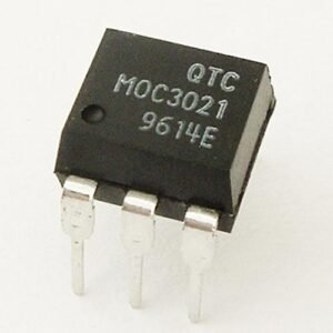
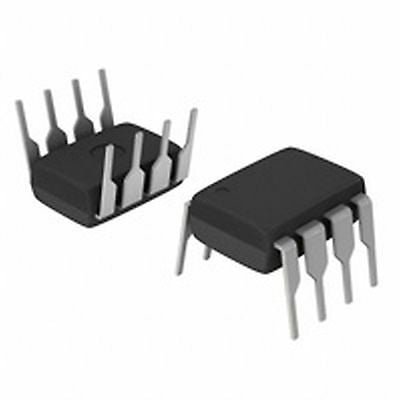
MOC3021 Triac Driven Optoisolator
Original price was: ₨150.00.₨69.00Current price is: ₨69.00. Quick View- Opto-isolator with Zero-Crossing Triac Driver
- Input LED Diode Forward Voltage: 1.15V
- LED Forward Latch Current: 15mA
- TRIAC output terminal voltage: 400V (max)
- TRIAC peak output current: 1A
- Available as 6-pin PDIP with and without M-suffix
-
-28%
74LS47 IC – Common Anode LED Driver
Original price was: ₨90.00.₨65.00Current price is: ₨65.00. Quick View74LS47 is a BCD to 7-segment decoder/driver IC. It accepts a binary coded decimal as input and converts it into a pattern to drive a seven-segment for displaying digits 0 to 9.
-
-8%

This Tri-state bi-directional transceiver utilize advanced silicon-gate CMOS technology and is intended for two-way asynchronous communication between data buses. They have high drive current outputs which enable high speed operation even when driving large bus capacitances. The circuit possess the low power consumption of CMOS circuitry, yet have speeds comparable to low power Schottky TTL circuits.
-

The TL494 device incorporates all the functions required in the construction of a pulse-width-modulation (PWM) control circuit on a single chip. Designed primarily for power-supply control, this device offers the flexibility to tailor the power-supply control circuitry to a specific application. The TL494 device contains two error amplifiers, an on-chip adjustable oscillator, a dead-time control (DTC) comparator, a pulse-steering control flip-flop, a 5-V, 5%-precision regulator, and output-control circuits.The TL494C device is characterized for operation from 0C to 70C. The TL494I device is characterized for operation from 40C to 85C.
-
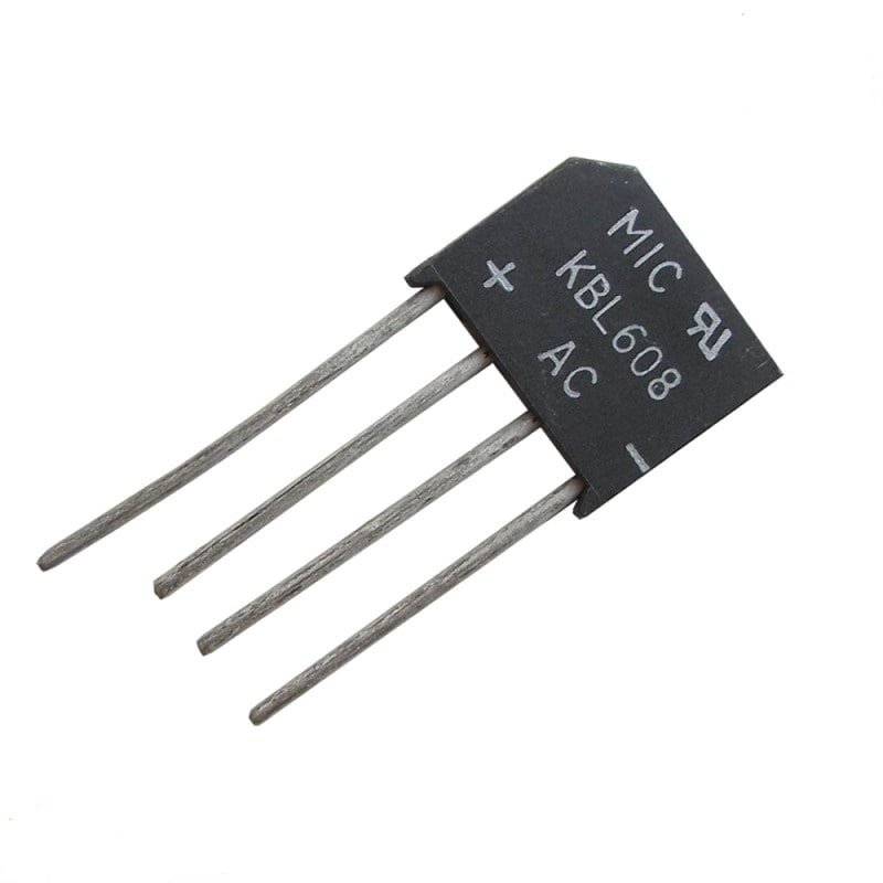
Bridge rectifier diode with a 6A current rating.
-

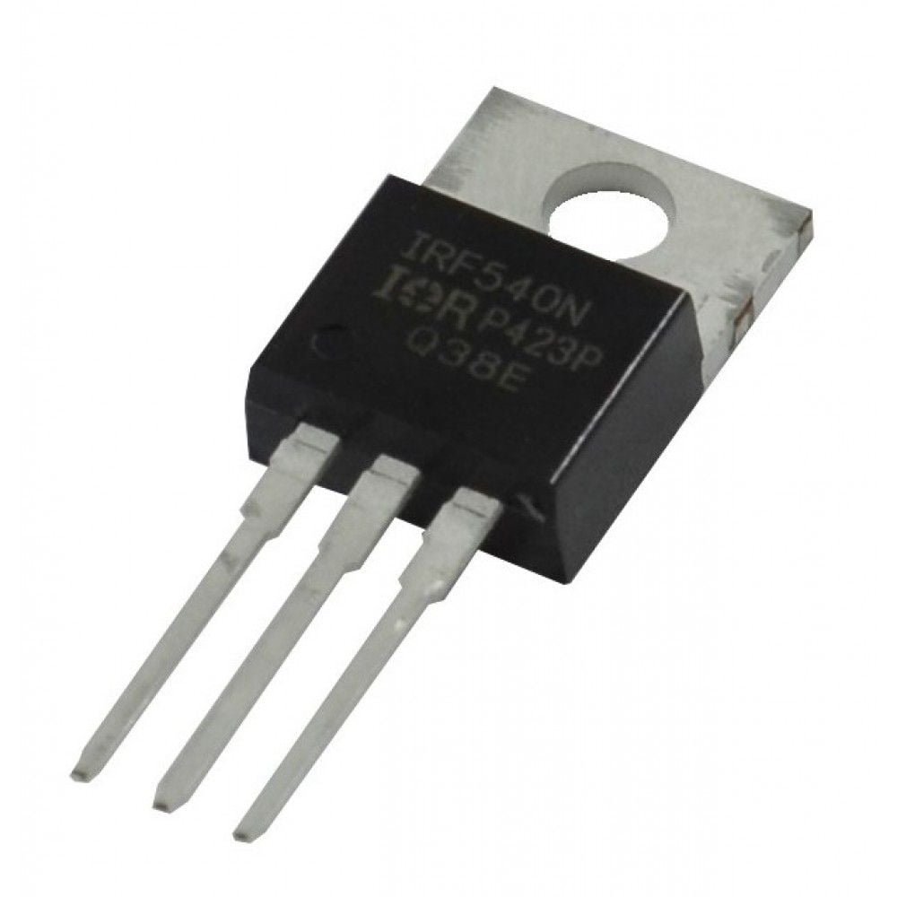
- N-Channel Power MOSFET
- Continuous Drain Current (ID): 10A
- Gate threshold voltage (VGS-th) is 10V (limit = 20V)
- Drain to Source Breakdown Voltage: 400V
- Drain Source Resistance (RDS) is 0.55 Ohms
- Rise time and fall time is 27nS and 24nS
- Available in To-220 package
-

- Low saturation voltage
- Simple drive requirements
- High safe operating area
- For low distortion complementary designs
- Easy to carry and handle
-
-16%
- Logic Type: INVERTER / NOR / NAND
- Output Current: 6.8mA
- Supply voltage range: 3V to 18V
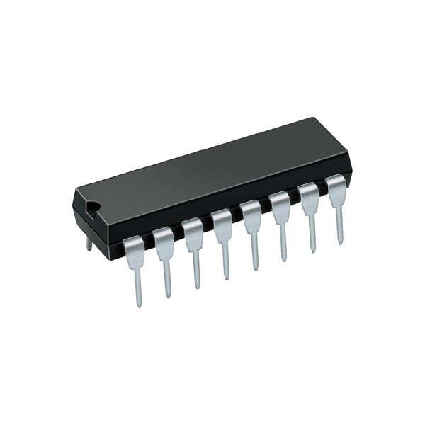
- Package Type: DIP
- Pin number: 14
- Operating temperature range: -55 ° C to +125 ° C
- Surface Mount Devices: through-hole mounting
-
-21%
SCR C106 C106 Series – SCR TO-255AA 4A
Original price was: ₨75.00.₨59.00Current price is: ₨59.00. Quick View- Glassivated Surface for Reliability and Uniformity
- Power Rated at Economical Prices
- Practical Level Triggering and Holding Characteristics
- Flat, Rugged, Thermopad Construction for Low Thermal Resistance, High Heat Dissipation and Durability
- Sensitive Gate Triggering
- Device Marking: Device Type, e.g., C106B, Date Cod
-
-19%
 Out Of Stock
The AD7528 is a monolithic dual 8-bit digital/analog converter featuring excellent DAC-to-DAC matching. It is available in skinny 0.3″ wide 20-lead DIPs and in 20-lead surface mount packages. Separate on-chip latches are provided for each DAC to allow easy microprocessor interface.
-

This Power MOSFET provides the circuit designer with the best combination of fast switching, ruggedized device design, low on-resistance and cost-effectiveness.
-

N-Channel Power MOSFET provide the circuit designer with the best combination of fast switching, ruggedized device design, low on-resistance and cost-effectiveness.
-
ULN2004 Features
- Output current (single output): 500mA (MAX.)
- High sustaining voltage output: 50V (MIN.)
- Output clamp diodes
- Inputs compatible with various types of logic
-
-15%
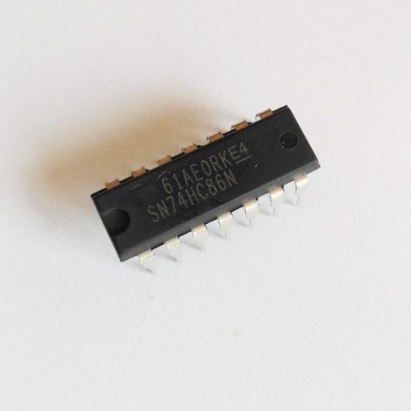
This device contains four independent gates each of which performs the logic exclusive-OR function.
-
-27%
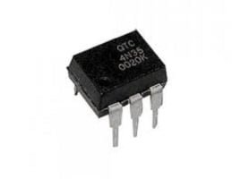
4N35 optocoupler consists of gallium arsenide infrared LED and a silicon NPN phototransistor.Isolation test voltage 5000 VRMS. Input-output coupling capacitance < 0.5 pF . 4N35 optocoupler consists of gallium arsenide infrared LED and a silicon NPN phototransistor.Isolation test voltage 5000 VRMS. Input-output coupling capacitance < 0.5 pF . 4N35 optocoupler consists of gallium arsenide infrared LED and a silicon NPN phototransistor.Isolation test voltage 5000 VRMS. Input-output coupling capacitance < 0.5 pF .
-
-20%

- Four individually operated voltage comparators
- Low noise interference among comparators
- Single Supply Operation: +3.0 V to +36 V
- Dual Supply Operation: +18V and -18V
- Low Input Bias Current: 25 nA
- Low Input Offset Current: 5.0 nA
- Low Input Offset Voltage
- Input Common Mode Voltage Range to GND
- Low Output Saturation Voltage: 130 mV @ 4.0 mA
- TTL and CMOS compatible
- ESD Clamps on the inputs increase reliability without affecting device operation
- Pb Free, Halogen Free/BFR Free and RoHS compliant
-
-21%
 Out Of Stock
- HP2730 Opto Coupler IC
- Number of Channels: 2
- Voltage – Isolation: 2500 Vrms
- Current Transfer Ratio (Min): 300% @ 1.6 mA
- Turn On / Turn Off Time (Typ): 300 ns, 5 s
- Input Type: DC
- Output Type: Darlington
- Voltage – Output (Max): 7 V
- Current – Output / Channel: 60 mA
- Voltage – Forward (Vf) (Typ): 1.3 V
- Current – DC Forward (If) (Max): 20 mA
- Operating Temperature: -40C to 85C
- Mounting Type: Through Hole
- Package: 8-DIP (0.300″, 7.62mm)
-

- Wide supply voltage range 3.0V to 15V
- Low power 10 nW (typ.)
- High noise immunity 0.45 VDD (typ.)
- Buffered Inputs and Outputs
- Standard Symmetrical Output Characteristics
- 100% Tested for Maximum Quiescent Current at 20V
- 5V, 10V and 15V Parametric Ratings
- Maximum Input Current of 1A at 18V Over Full Package-Temperature Range; 100nA at 18V and +25oC
-
- Fast Switching Applications
- Uninterruptible Power Supplies
- Battery Chargers
- Battery Management Systems
- Solar Battery Chargers
- Solar Uninterruptible Power Supplies
- Motor Driver Applications
- Telecommunication Applications
- Computer Related Applications
-
-30%

CD4051 Single 8-channel Multiplexer Demultiplexer
Original price was: ₨70.00.₨49.00Current price is: ₨49.00. Quick View- Analog and Digital Multiplexing and Demultiplexing
- A/D and D/A Conversion
- Signal Gating
- Factory Automation
- Televisions
- Appliances
- Consumer Audio
- Programmable Logic Circuits
- Sensors
-
-18%
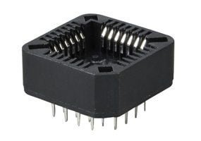
This is a IC Socket/Base for 28 pin SMD PLCC IC. This is a SMT base and is advisable on boards with point to point wiring because replacing a defective IC is time consuming and can possibly damage your prototype board. The use of an IC socket is inexpensive compared to the time and effort required to replace an IC chip. IC sockets also reduce the possibility of damaging the board when swapping out IC’s.
-
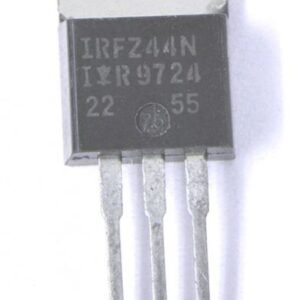
- Package Type: TO-220
- Transistor Type: N Channel
- Max Voltage Applied From Drain to Source: 55V
- Max Gate to Source Voltage Should Be: 20V
- Max Continues Drain Current is : 49A
- Max Pulsed Drain Current is: 160A
- Max Power Dissipation is: 94W
- Minimum Voltage Required to Conduct: 2V to 4V
- Max Storage & Operating temperature Should Be: -55 to +170 Centigrade
-

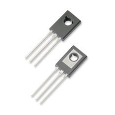
The Bipolar Power Transistor is designed for use in general purpose amplifier and switching applications.
-
-25%
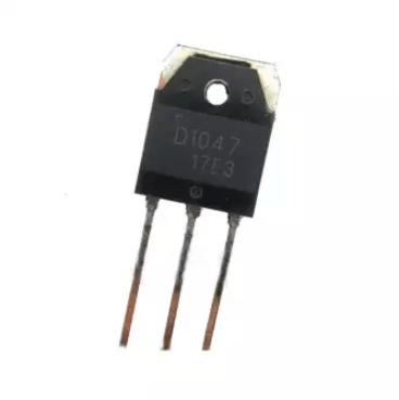
2SD1047 Bipolar NPN type Transistor.
-
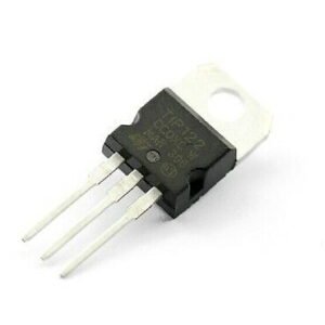
TIP122 transistor designed for general purpose amplifier and low speed switching applications.
-
-18%
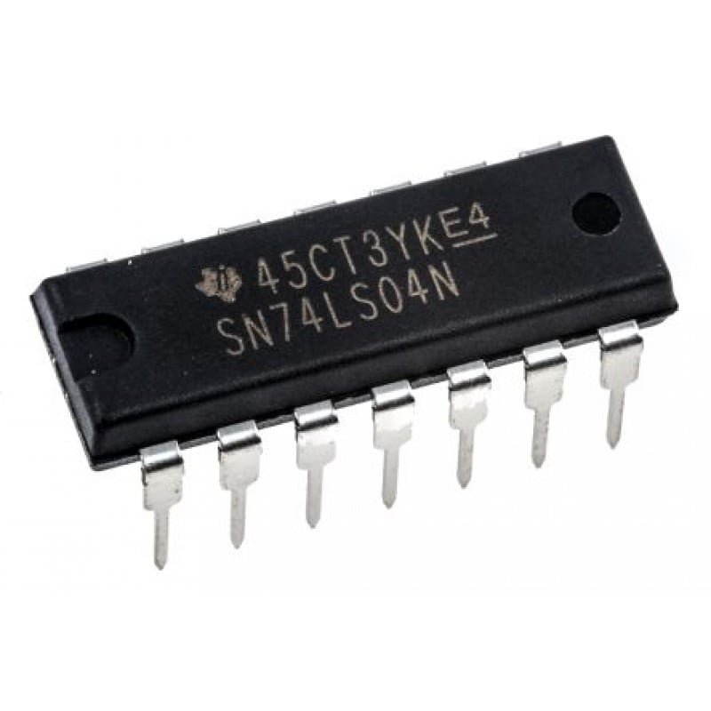
- HEX Inverter
- Logic Gate IC
- Not Gate | Inverter
- 7404
- SN74HC04N same as SN74LS04N
- IC 04 IC04
-
-18%
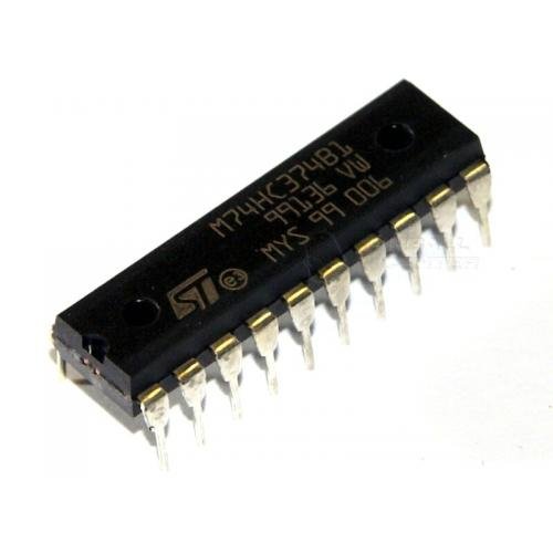
A flip flop is a device that is able to store single bit of data. It is either one or zero, off or on in this case. It is able to store data over a prolonged period of time. There are many applications of 74HC374 Flip Flop IC.
-
-18%

- Identical in Function to the 74LS93 with Different Pin Arrangement
- Contains Four Master-Slave Flips-Flops together with a Binary Counter
- Gated Zero Reset
- Fast Propagation Speeds
- Low Power Dissipation
-
-11%
SN74125 Buffer & Line Driver IC
Original price was: ₨55.00.₨49.00Current price is: ₨49.00. Quick View- Technology Family: LS
- VCC (Min): 4.75V
- VCC (Max): 5.25
- Channels (#): 4
- Operating Voltage (Nom): 5V
- Frequency at normal voltage (Max): 35MHz
- Propagation delay (Max): 20ns
- IOL (Max): 24mA
- IOH (Max):-2.6mA
- Input Type: Bi-polar
- Output type: 3-State
- High speed (tpd 10-50ns)
- Rating: Catalog
- Data rate: 70Mbps
- Available in 14-pin PDIP, GDIP, PDSO packages
-
-46%
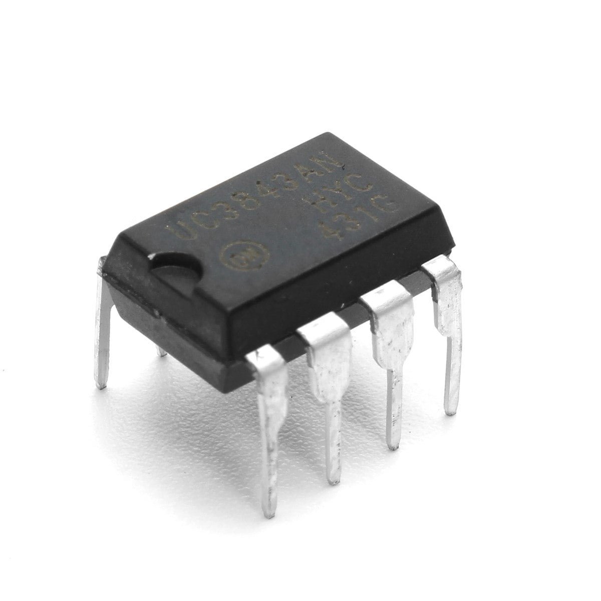
- Current-Mode PWM controller
- Operating Voltage: 7.0V to 8.2V
- Output pin current: 1A
- Analog input range: -0.3 to 6.3V
- Oscillation Frequency: 52 Typically
- Gain: 3V
- Maximum source current: 22mA
- Low Output Voltage: 0.08V
- High Output Voltage: 13.5V
-
- Supply voltage ranges from 3v to 18v
- Set-up-time is 150, 70, and 40ns at 5v, 10v, and 15v respectively
- Strobe pulse width is 400, 160, and 100ns at 5v, 10v, and 15v respectively
- Hold time is zero
- 100% tested for quiescent current at 20v
- Having high input current of 1uA (max.) at 18v
- Maximum output current sourcing of 25mA
- Operating temperature ranges from -40 C to 85 C
- Storage temperature ranges from -65 C to 150 C
-
The 74LS373 consists of eight latches with 3-state outputs for bus organized system applications. The flip-flops appear transparent to the data.
-
This NPN Bipolar Darlington Transistor is designed for use in switching applications, such as print hammer, relay, solenoid and lamp drivers.
-
The Exclusive OR gates are monolithic complementary MOS (CMOS) integrated circuits constructed with N-Channel and P-Channel enhancement mode transistors. All inputs are protected against static discharge with diodes to VDD and VSS.
-
- Wide supply voltage range: 3V to 15V
- Low power: 100 nW (typ.)
- High noise immunity: 0.45 VDD (typ.)
- Separate SET and RESET inputs for each latch
- NOR and NAND configuration
- 3-STATE output with common output enable
-
The 4077 is a quad 2-input EXCLUSIVE-NOR gate. The outputs are fully buffered for the highest noise immunity and pattern insensitivity to output impedance. The 4077 operates over a recommended VDD power supply range of 3 V to 15 V referenced to VSS (usually ground). Unused inputs must be connected to VDD, VSS, or another input.
-
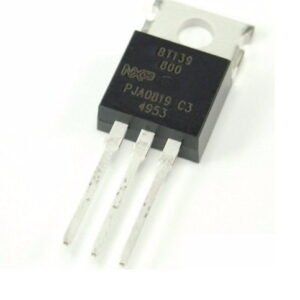
The BT139 is a TRIAC thyristor, which is a type of semiconductor device that can use to control alternating current (AC) power. TRIAC thyristor BT139 is a four-quadrant device, meaning that it can conduct current in either direction. The BT139 has a peak inverse voltage (PIV) of 800 volts and a current rating of 16 amperes. It is a sensitive gate triac, meaning that it can be triggered with a low gate current. The on-state voltage drop of the BT139 is 1.2 volts. Here are some of the key features of the BT139-800E 4 Quadrant TRIAC:
- Peak inverse voltage (PIV): 800 V
- RMS current: 16 A
- Gate trigger current: 2.5 mA
- Gate trigger voltage: 1.4 V
- On-state voltage drop: 1.2 V
- Thermal resistance: 1.2 K/W (junction to mounting base)
- Operating temperature range: -40 to 125 °C
-
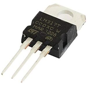
The LM317 device is an adjustable three-terminal positive-voltage regulator capable of supplying more than 1.5 A over an output-voltage range of 1.25 V to 37 V. It requires only two external resistors to set the output voltage. The device features a typical line regulation of 0.01% and typical load regulation of 0.1%. It includes current limiting, thermal overload protection, and safe operating area protection. Overload protection remains functional even if the ADJUST terminal is disconnected.
-
-33%
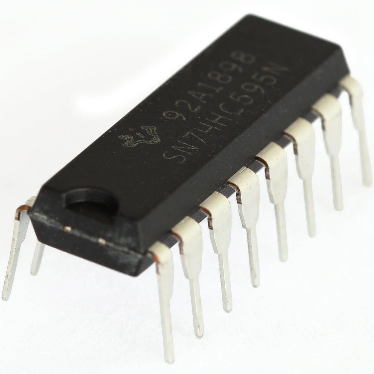
74HC595 74HC595D Shift Register
Original price was: ₨60.00.₨40.00Current price is: ₨40.00. Quick View74HC595 8-BIT SERIAL-IN SERIAL OR PARALLEL-OUT SHIFT REGISTER contain an 8-bit serial-in, parallel-out shift register that feeds an 8-bit D-type storage register. The storage register has parallel 3-state outputs. Separate clocks are provided for both the shift and storage register. The shift register has a direct overriding clear (SRCLR) input, serial (SER) input, and serial outputs for cascading. When the output-enable (OE) input is high, the outputs are in the high-impedance state.
-
-33%

D-Type Flip-Flop 74HC175 DIP16 – SN74HC175N
Original price was: ₨60.00.₨40.00Current price is: ₨40.00. Quick View- Outputs can drive up to 10 LSTTL loads
- Contain four flip-flops with double-rail outputs
- 80A Maximum low power consumption
- 13ns Typical tpd
- 4mA Output drive at 5V
- 1A Maximum low input current
-
-33%
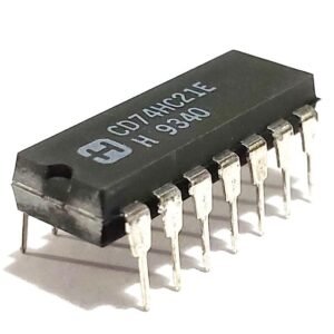
CD74HC21E 74HC21 Dual 4-Input Positive-AND Gates IC
Original price was: ₨60.00.₨40.00Current price is: ₨40.00. Quick View- Wide Operating Voltage Range of 2 V to 6 V
- Outputs Can Drive Up To 10 LSTTL Loads
- Low Power Consumption, 20-?A Max ICC
- Typical tpd= 11 ns
- ?4-mA Output Drive at 5 V
- Low Input Current of 1 ?A Max
-
-20%
 Out Of Stock
K2045 Mosfet 2SK2045 TO-220F FET K2045 NPN
Original price was: ₨50.00.₨40.00Current price is: ₨40.00. Quick ViewLow ON resistance. Ultrahigh-speed switching. High-speed diode built in.
-

74HC540 is a 20 Pin Octal 3-state Inverting Buffer IC having 2V to 6V Operating Voltage range with 6mA output current. The 3-STATE buffers utilize advanced silicon-gate CMOS technology. They possess high drive current outputs which enable high speed operation even when driving large bus capacitances.
-

The 7408 is a QUAD 2-Input AND gates and contains four independent gates each of which performs the logic AND function. It comes in 14-pin DIP package. 7408 AND Gate IC 74HC244 74244 Octal Buffers & Line Driver IC in Pakistan
-
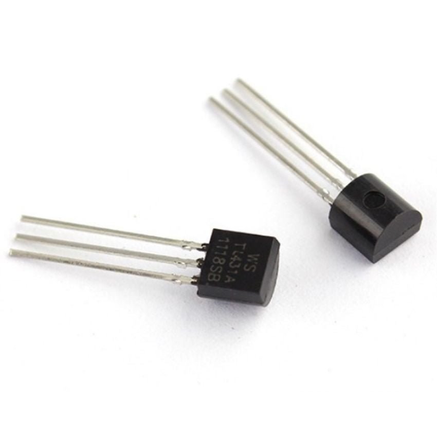
The TL431 is three-terminal adjustable shunt regulators, with specified thermal stability over applicable automotive, commercial, and military temperature ranges. The output voltage can be set to any value between Vref (approximately 2.5 V) and 36 V, with two external resistors. These devices have a typical output impedance of 0.2 .
-

- Inverting IC that can convert High logic level to Low level
- High source and Sink Current as it has the capability of driving 2 TTL Loads at 5V over full temperature range.
- 100% Tested for Quiescent Current at 20 V
- Maximum Input Current of 1A at 18 V Over Full Package Temperature Range; 100 nA at 18 V and 25C
- 5-V, 10-V, and 15-V Parametric Ratings
- It is available in 16 pin packages of PDIP, SOIC, TSSOP, SO.
- Special input protection to protect inputs against static discharges.
-
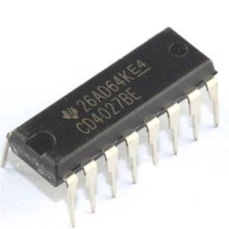
- CD4027 Dual JK Flip Flop Package IC which operates at medium speed of 16 MHz typically with 10V supply
- Voltage range of 3.0V to 15V
- Static Flip-Flop Operation
- High noise immunity of 0.45 VDD(typ.)
- Set and Reset capability
- TTL compatible
- Low power of 50 nW (typ.)
- Input Rise/Fall time at 5V: 45us
- Maximum and minimum Input Voltage is 2 V and 0.8 V
-
The CD4081 quad gate is a monolithic complementary MOS (CMOS) integrated circuit constructed with N- and P-channel enhancement mode transistors. They have equal source and sink current capabilities and conform to standard B series output drive. The devices also have buffered outputs which improve transfer characteristics by providing very high gain. All inputs protected against static discharge with diodes to VDD and VSS.