-
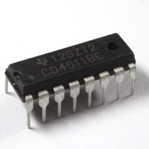
- Supply voltage ranges from 3v to 18v
- Set-up-time is 150, 70, and 40ns at 5v, 10v, and 15v respectively
- Strobe pulse width is 400, 160, and 100ns at 5v, 10v, and 15v respectively
- Hold time is zero
- 100% tested for quiescent current at 20v
- Having high input current of 1uA (max.) at 18v
- Maximum output current sourcing of 25mA
- Operating temperature ranges from -40 C to 85 C
- Storage temperature ranges from -65 C to 150 C
-
-18%
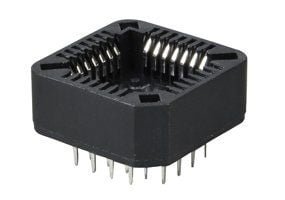
This is a IC Socket/Base for 28 pin SMD PLCC IC. This is a SMT base and is advisable on boards with point to point wiring because replacing a defective IC is time consuming and can possibly damage your prototype board. The use of an IC socket is inexpensive compared to the time and effort required to replace an IC chip. IC sockets also reduce the possibility of damaging the board when swapping out IC’s.
-
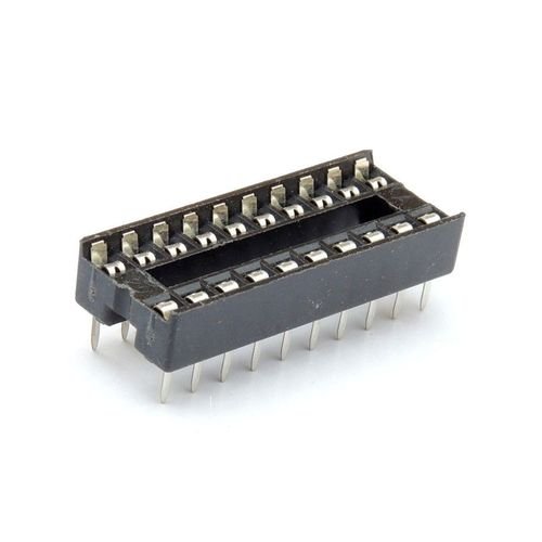
IC sockets are generally for preventing damage to IC’s from soldering and while testing multiple circuits. These are made from Black Thermoplastic and tin-plated alloy contacts. One end is notched to aid in identification. They can be mounted end to end to suit longer IC’s.
-
-14%
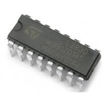
L293D IC Dual H-Bridge Motor Driver
Original price was: ₨150.00.₨129.00Current price is: ₨129.00. Quick View- It can be used to run Two DC motors with the same IC.
- Speed and Direction control is possible
- Motor driver voltage Vcc2 (Vs): 4.5V to 36V
- Maximum Peak motor current: 1.2A
- Maximum Continuous Motor Current: 600mA
- Supply Voltage to Vcc1(VSS): 4.5V to 7V
- Transition time: 300ns (at 5Vand 24V)
- Automatic Thermal shutdown is available
- Available in 16-pin DIP, TSSOP, SOIC packages
-
-18%
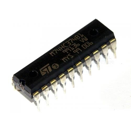
A flip flop is a device that is able to store single bit of data. It is either one or zero, off or on in this case. It is able to store data over a prolonged period of time. There are many applications of 74HC374 Flip Flop IC.
-
-11%
SN74125 Buffer & Line Driver IC
Original price was: ₨55.00.₨49.00Current price is: ₨49.00. Quick View- Technology Family: LS
- VCC (Min): 4.75V
- VCC (Max): 5.25
- Channels (#): 4
- Operating Voltage (Nom): 5V
- Frequency at normal voltage (Max): 35MHz
- Propagation delay (Max): 20ns
- IOL (Max): 24mA
- IOH (Max):-2.6mA
- Input Type: Bi-polar
- Output type: 3-State
- High speed (tpd 10-50ns)
- Rating: Catalog
- Data rate: 70Mbps
- Available in 14-pin PDIP, GDIP, PDSO packages
-
-25%
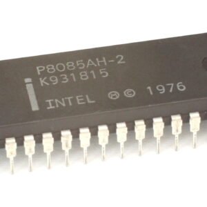
The 8085 is an 8-bit general purpose microprocessor that can address 64K Byte of memory. It has 40 pins and uses +5V for power. It can run at a maximum frequency of 3 MHz.
-
-13%

- Ultra Low Power Consumption 0.7 μA
- Wide Range of Supply Voltages 2V to 8V
- Input Common-Mode Range Beyond V+ and V−
- Open Collector and Push-Pull Output
- High Output Current Drive: (@ VS = 5V) 45 mA
- Propagation Delay (@ VS = 5V, 10 mV Overdrive) 25 μs
- Tiny 5-Pin SOT-23 Package
- Latch-up Resistance >300 mA
- LMC7215-Q1 is an Automotive Grade Product that is AEC-Q100 Grade 3 Qualified.
-
-20%
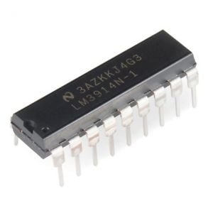
- Analog Controlled LED Driver IC
- Number of controllable LEDs: 10
- Operating Voltage: 3V to 18V
- Input Analog voltage range: 1.2V to 12V
- LED sink current: 2mA to 30mA (programmable)
- Both Dot/Bar mode available
- Can be cascaded to control upto 100 LEDs
- Available in 18-pin DIP package
-
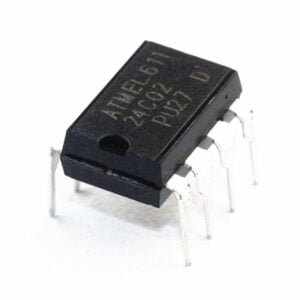
- Low-voltage and Standard-voltage Operation
- 2.7 (VCC = 2.7V to 5.5V)
- 1.8 (VCC = 1.8V to 5.5V)
- Internally Organized 128 x 8 (1K), 256 x 8 (2K), 512 x 8 (4K),
- 1024 x 8 (8K) or 2048 x 8 (16K)
- Two-wire Serial Interface
- Schmitt Trigger, Filtered Inputs for Noise Suppression
- Bidirectional Data Transfer Protocol
- 100 kHz (1.8V) and 400 kHz (2.7V, 5V) Compatibility
- Write Protect Pin for Hardware Data Protection
- 8-byte Page (1K, 2K), 16-byte Page (4K, 8K, 16K) Write Modes
- Partial Page Writes Allowed
- Self-timed Write Cycle (5 ms max)
- High-reliability
- Endurance: 1 Million Write Cycles
- Data Retention: 100 Years
- Automotive Devices Available
- 8-lead JEDEC PDIP, 8-lead JEDEC SOIC, 8-lead Ultra Thin Mini-MAP (MLP 2×3), 5-lead SOT23, 8-lead TSSOP and 8-ball dBGA2 Packages
- Die Sales: Wafer Form, Waffle Pack and Bumped Wafers
- Low-voltage and Standard-voltage Operation
-
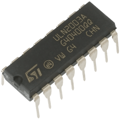
- Seven Darlingtons per package
- Output current 500 mA per driver (600 mA peak)
- Output voltage 50 V
- Integrated suppression diodes for inductive loads
- Outputs can be paralleled for higher current
- TTL/CMOS/PMOS/DTL compatible inputs
- Inputs pinned opposite outputs to simplify
-

The DS1307 serial real-time clock (RTC) is a lowpower, full binary-coded decimal (BCD) clock/calendar plus 56 bytes of NV SRAM. Address and data are transferred serially through an I2C, bidirectional bus. The clock/calendar provides seconds, minutes, hours, day, date, month, and year information. The end of the month date is automatically adjusted for months with fewer than 31 days, including corrections for leap year. The clock operates in either the 24-hour or 12-hour format with AM/PM indicator. The DS1307 has a built-in power-sense circuit that detects power failures and automatically switches to the backup supply. Timekeeping operation continues while the part operates from the backup supply.
-
-51%

DS1302 is a tickle-charge timekeeping chip which contains a real-time clock/calendar and 31 bytes of static RAM. DS1302 uses serial communication to interact with microcontrollers. Also, it automatically adjust the date for the month with fewer days. Clock operates in 24hr or 12hr format with an AM/PM indicator. DS1302 chip is also commonly used as DS1302 RTC module which comes with a 32 kHz crystal and on-board battery backup all in a small SIP module that is compatible with a breadboard. DS1302 module are used by makers with Arduino, Raspberry Pi and other Micro-controllers.
-
-20%
The uA723 is a precision integrated-circuit voltage regulator, featuring high ripple rejection, excellent input and load regulation, excellent temperature stability, and low standby current. The circuit consists of a temperature-compensated reference-voltage amplifier, an error amplifier, a 150-mA output transistor, and an adjustable-output current limiter.The uA723 is characterized for operation from 0C to 70C.
-

The TL494 device incorporates all the functions required in the construction of a pulse-width-modulation (PWM) control circuit on a single chip. Designed primarily for power-supply control, this device offers the flexibility to tailor the power-supply control circuitry to a specific application. The TL494 device contains two error amplifiers, an on-chip adjustable oscillator, a dead-time control (DTC) comparator, a pulse-steering control flip-flop, a 5-V, 5%-precision regulator, and output-control circuits.The TL494C device is characterized for operation from 0C to 70C. The TL494I device is characterized for operation from 40C to 85C.
-
-31%
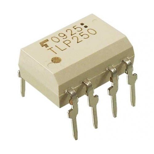
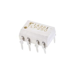
TLP250 MOSFET IGBT DRIVER TLP-250
Original price was: ₨360.00.₨249.00Current price is: ₨249.00. Quick View- Input threshold current: IF=5mA(max.)
- Supply current (ICC): 11mA(max.)
- Supply voltage (VCC): 1035V
- Output current (IO): 1.5A (max.)
- Switching time (tpLH/tpHL): 1.5s(max.)
- Isolation voltage: 2500Vrms(min.)
- UL recognized: UL1577, file No.E67349
- Option (D4) type
- VDE approved: DIN VDE0884/06.92,certificate No.76823
- Maximum operating insulation voltage: 630VPK
- Highest permissible over voltage: 4000VPK
- Creepage distance: 6.4mm(min.)
- Clearance: 6.4mm(min.)
-
-20%
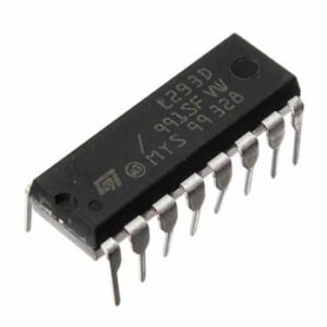
L293D L293-D Dual H-Bridge Motor Driver
Original price was: ₨150.00.₨120.00Current price is: ₨120.00. Quick View- Can drive 2 DC motors simultaneously in either direction
- Wide voltage supply range: 4.5V to 36V
- Separate input-logic supply
- Internal ESD protection
- High-noise-immunity inputs
- Thermal shutdown
- Output clamp diodes for inductive transient suppression
-
-8%

L293E Push-Pull Four Channel Drivers
Original price was: ₨240.00.₨220.00Current price is: ₨220.00. Quick View- OVERTEMPERATURE PROTECTION
- OUTPUT CURRENT 1A PER CHANNEL
- INHIBIT FACILITY
- PEAK OUTPUT CURRENT 2A PER CHANNEL (non repetitive)
- SEPARATE LOGIC SUPPLY
- HIGH NOISE IMMUNITY
-
-27%
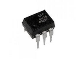
4N35 optocoupler consists of gallium arsenide infrared LED and a silicon NPN phototransistor.Isolation test voltage 5000 VRMS. Input-output coupling capacitance < 0.5 pF . 4N35 optocoupler consists of gallium arsenide infrared LED and a silicon NPN phototransistor.Isolation test voltage 5000 VRMS. Input-output coupling capacitance < 0.5 pF . 4N35 optocoupler consists of gallium arsenide infrared LED and a silicon NPN phototransistor.Isolation test voltage 5000 VRMS. Input-output coupling capacitance < 0.5 pF .
-
-8%
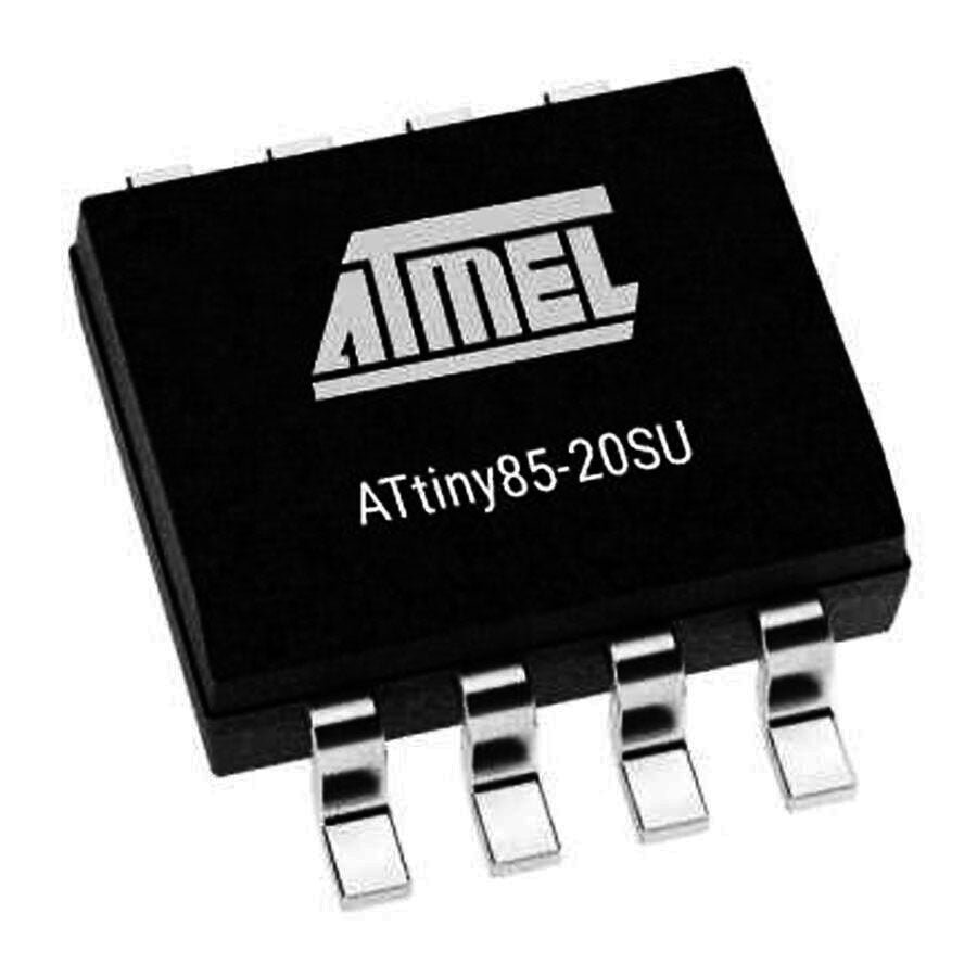
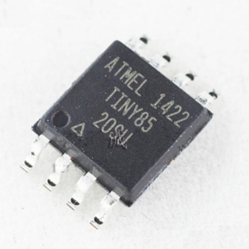
Atmel Attiny85 Attiny-85 ATtiny85-20PU
Original price was: ₨1,200.00.₨1,099.00Current price is: ₨1,099.00. Quick ViewFeatures of ATtiny85 Microcontroller:-
- Flash (Kbytes): 8 Kbytes
- Pin Count: 8
- Max. Operating Freq. (MHz): 20 MHz
- CPU: 8-bit AVR
- Number of Touch Channels: 3
- Hardware QTouch Acquisition: No
- Max I/O Pins: 6
- Ext Interrupts: 6
- USB Interface:No
- Package – SMD
-
-20%
 Out Of Stock
 -
-13%
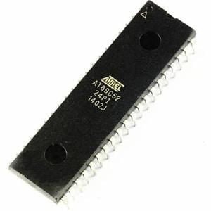
The AT89C52 is a lowe power, high performance CMOS 8-bit microcontroller with 8K bytes of Flash programmable and reaseable read only memory (PEROM). The on-chip flash allows the program memory to be reprogrammed in-syetem.
-
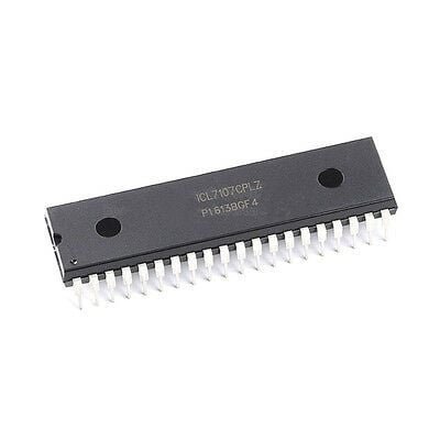
- Guaranteed zero reading for 0 V input on all scales
- True polarity at zero for precise null detection
- 1pA typical input current
- True differential input and reference, direct display drive – LED lCL7107
- Low noise – less than 15 VP-P
- On-chip clock and reference
- Low power dissipation – typically less than 10mW
- No additional active circuits required
- Enhanced display stability
- Pb-free (RoHS compliant)
-
-20%
 Out Of Stock
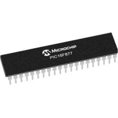
PIC 16F877 Microcontroller
Original price was: ₨1,500.00.₨1,199.00Current price is: ₨1,199.00. Quick ViewThis robust (200 nanosecond instruction execution) yet easy-to-program (only 35 single word instructions) CMOS FLASH-based 8-bit microcontroller packs Microchip’s robust PIC® architecture into a 40- or 44-pin package. It is upwards compatible with the PIC16C5X, PIC12CXXX and PIC16C7X devices. The PIC16F877A features 256 bytes of EEPROM data memory, self-programming, an ICD, 2 Comparators, 8 channels of 10-bit Analog-to-Digital (A/D) converter, 2 capture/compare/PWM functions, the synchronous serial port can be configured as either 3-wire Serial Peripheral Interface (SPI™) or the 2-wire Inter-Integrated Circuit (I²C™) bus and a Universal Asynchronous Receiver Transmitter (USART). These features make it ideal for more advanced level A/D applications in automotive, industrial, appliances and consumer applications.
-
-19%
 Out Of Stock
The AD7528 is a monolithic dual 8-bit digital/analog converter featuring excellent DAC-to-DAC matching. It is available in skinny 0.3″ wide 20-lead DIPs and in 20-lead surface mount packages. Separate on-chip latches are provided for each DAC to allow easy microprocessor interface.
-
-21%
 Out Of Stock
- HP2730 Opto Coupler IC
- Number of Channels: 2
- Voltage – Isolation: 2500 Vrms
- Current Transfer Ratio (Min): 300% @ 1.6 mA
- Turn On / Turn Off Time (Typ): 300 ns, 5 s
- Input Type: DC
- Output Type: Darlington
- Voltage – Output (Max): 7 V
- Current – Output / Channel: 60 mA
- Voltage – Forward (Vf) (Typ): 1.3 V
- Current – DC Forward (If) (Max): 20 mA
- Operating Temperature: -40C to 85C
- Mounting Type: Through Hole
- Package: 8-DIP (0.300″, 7.62mm)
-
-28%
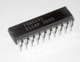
SN74HC241 Buffer & Line Driver IC
Original price was: ₨250.00.₨180.00Current price is: ₨180.00. Quick ViewThese octal buffers and line drivers are designed specifically to improve both the performance and density of 3-state memory address drivers, clock drivers, and bus-oriented receivers and transmitters. The HC241 devices are organized as two 4-bit buffers/drivers with separate output-enable (1OE and 2OE) inputs. When 1OE is low or 2OE is high, the device passes noninverted data from the A inputs to the Y outputs. When 1OE is high or 2OE is low, the outputs for the respective buffers/drivers are in the high-impedance state.
-
-22%
 Out Of Stock
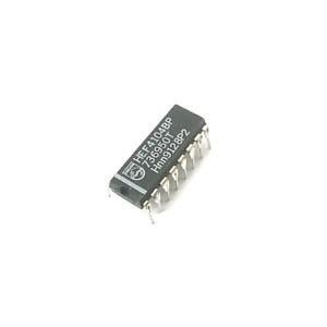
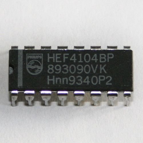
The HEF4104B is a quad low voltage-to-high voltage translator with 3-state outputs. It provides the capability of interfacing low voltage circuits to high voltage circuits. For example low voltage Local Oxidation Complementary MOS (LOCMOS) and Transistor-Transistor Logic (TTL) to high voltage LOCMOS. It has four data inputs (A0 to A3), an active HIGH output enable input (OE), four data outputs (B0 to B3) and their complements (B0 to B3).
-
-33%
- Output current (single output): 500 mA (max)
- High sustaining voltage output: 50 V (min)
- Output clamp diodes
- Inputs compatible with various types of logic.
- Package type-AFG: SOP-18 pin
-
 Out Of Stock
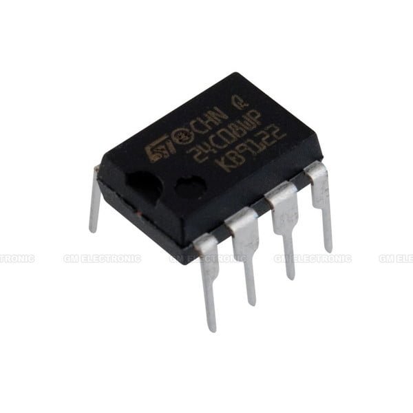
The M24C08 is an 8-Kbit I2C-compatible EEPROM (Electrically Erasable PROgrammable Memory) organized as 1 K 8 bits. It operate with a clock frequency of 400 kHz.
-
-20%
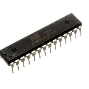
ATMEGA 328P ATMEGA328P-PU MICROCONTROLLER
Original price was: ₨1,500.00.₨1,199.00Current price is: ₨1,199.00. Quick ViewThe ATMEGA328P-PU is a low-power CMOS 8-bit microcontroller based on the AVR enhanced RISC architecture. By executing powerful instructions in a single clock cycle, the ATmega328P-PU achieves throughputs approaching 1 MIPS per MHz allowing the system designer to optimize power consumption versus processing speed.
The AVR core combines a rich instruction set with 32 general purpose working registers. All the 32 registers are directly connected to the Arithmetic Logic Unit (ALU),allowing two independent registers to be accessed in one single instruction executed in one clock cycle. The resulting architecture is more code efficient while achieving throughputs up to ten times faster than conventional CISC microcontrollers.The ATmega328P-PU AVR is supported with a full suite of program and system development tools including: C Compilers, Macro Assemblers, Program Debugger/Simulators, In-Circuit Emulators, and Evaluation kits.