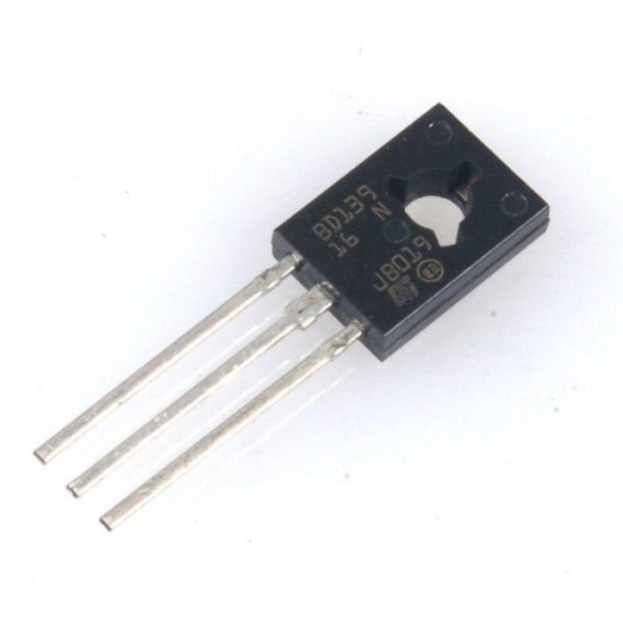
BD139 Transistor Overview
BD139 is a NPN transistor hence the collector and emitter will be left open (Reverse biased) when the base pin is held at ground and will be closed (Forward biased) when a signal is provided to base pin
BD139 has a gain value of 40 to 160, this value determines the amplification capacity of the transistor. The maximum amount of current that could flow through the Collector pin is 1.5A, hence we cannot connect loads that consume more than 1.5A using this transistor. To bias a transistor we have to supply current to base pin, this current (IB) should be limited to 1/10th of the collector current and voltage across the base emitter pin should be 5V maximum.
When this transistor is fully biased then it can allow a maximum of 1.5A to flow across the collector and emitter. This stage is called Saturation Region and the typical voltage allowed across the Collector-Emitter (VCE) or Base-Emitter (VBE) could be 80V. When base current is removed the transistor becomes fully off, this stage is called as the Cut-off Region.
The BD139 was originally manufactured by Phillips rated at 160MHz for specific audio applications, later they were cloned by other manufacturers like Samsung, ST etc.
Features
- Plastic casing NPN Transistor
- Continuous Collector current (IC) is 1.5A
- Collector-Emitter voltage (VCE) is 80 V
- Collector-Base voltage (VCB) is 80V
- Base Current (Ib) is 0.5A
- Emitter Base Breakdown Voltage (VBE) is 5V
- DC current gain (hfe) is 40 to 160
- Available in To-225 package

Reviews
There are no reviews yet.