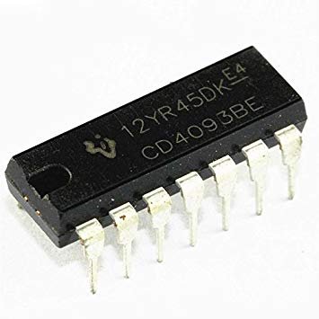
CD4093 – Quad 2-Input NAND Schmitt Triggers
CD4093 – Quad 2-Input NAND Schmitt Triggers is also called a quad package 2-input NAND gate as it contains four independent 2-Input NAND gates with Schmitt trigger action. The IC is operated on different voltage levels and can consume a maximum of 1uA current when operated at 18V DC.
Features and Specifications
This section mentions some of the features and specifications of the CD4093 IC.
- Operating Voltage: 5V, 10V, 15V DC
- Maximum Input Current: 1uA
- Hysteresis Voltage Typically 0.9 V at VDD: 5 V and 2.3 V at VDD: 10 V
- Noise Immunity Greater Than 50%
- Unlimited input rise and fall times
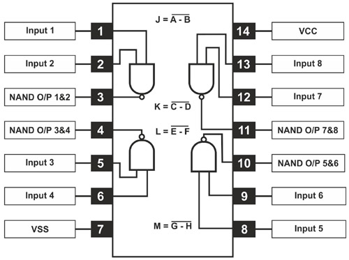
Pin Configuration
The IC has 14 pins for I/O and power. The IC has four Schmitt trigger circuits with 2 input NAND gates, the table below gives us a clearer understanding of the pin configuration of the IC.
|
Pin Number |
Pin Type |
Pin Description |
|
1 |
A |
Input 1 |
|
2 |
B |
Input 2 |
|
3 |
J |
NAND Output of A & B |
|
4 |
K |
NAND Output of C & D |
|
5 |
C |
Input 3 |
|
6 |
D |
Input 4 |
|
7 |
VSS |
Ground |
|
8 |
E |
Input 5 |
|
9 |
F |
Input 6 |
|
10 |
L |
NAND Output of E & F |
|
11 |
M |
NAND Output of G & H |
|
12 |
G |
Input 7 |
|
13 |
H |
Input 8 |
|
14 |
VCC |
Positive Voltage input |
Working and Output Table
Also known as the NOT-AND gate, it is the logic gate that provides a false output when the inputs are true, thus saying that it is the complement output of AND gate. The CD4093 is a 14 pin IC accommodation with 4 NAND gates internally. Pin(1) A and Pin(2) B are the inputs of the NAND gate 1 which provide a complement output of AND gate at pin(3) J. Similarly, the image below represents how the NAND gates are connected to which pins.
The truth table below shows the inputs and the output of the NAND gate. Any inputs provided to pin 1, 2, 5, 6, 8, 9, 11, 12, a corresponding output through the NAND gate will be received. The following table can be referred to for the input and output values.
|
Input A |
Input B |
Output |
|
0 |
0 |
1 |
|
1 |
0 |
1 |
|
0 |
1 |
1 |
|
1 |
1 |
0 |


Reviews
There are no reviews yet.