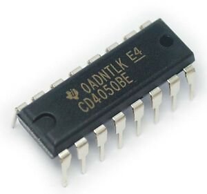
CD4050 Hex Non-Inverting IC Buffer/Converter
CD4050 Hex Non-Inverting IC Buffer/Converter consists of six individual non-inverting buffers. The IC can be used to drive up to two DTL or TTL devices at a time. The IC can be used as hex buffers, CMOS current drivers or as CMOS to DTL/ TTL converters.
Features and Specification
This section mentions some of the features and specifications of the Up counter IC.
- Operating Voltage: 3V – 15V DC
- Current consumption(max): 50mA
- High Sink Current for Driving 2 TTL Loads
- Maximum low-level output Voltage: 0.5V at 5V VCC
- Minimum high-level output voltage: 4.95 at 5V VCC
Note: More technical information can be found in the CD4050 Datasheet
CD4050 Pinout Configuration
The non-inverting IC consists of 16 pins for I/O and power. The table below can be referred to understand the pin configuration of the IC.
| Pin Number | Pin Type | Description/Direction |
| 1 | VCC | Positive input supply |
| 2 | G | Non-Inverted output 1 |
| 3 | A | Input 1 |
| 4 | H | Non-Inverted output 2 |
| 5 | B | Input 2 |
| 6 | I | Non-Inverted output 3 |
| 7 | C | Input 3 |
| 8 | VSS | Negative Supply |
| 9 | D | Input 4 |
| 10 | J | Non-Inverted output 4 |
| 11 | E | Input 5 |
| 12 | K | Non-Inverted output 5 |
| 13 | NC | No connection |
| 14 | F | Input 6 |
| 15 | L | Non-Inverted output 6 |
| 16 | NC | No connection |
Working and Use of a Non-Inverter IC
A non-inverting buffer IC consists of non-inverters that pass the input unchanged to its output. The Non-inverter works in the opposite way of the inverter IC. The IC’s main purpose is to regenerate the input, using a strong HIGH and a strong LOW.
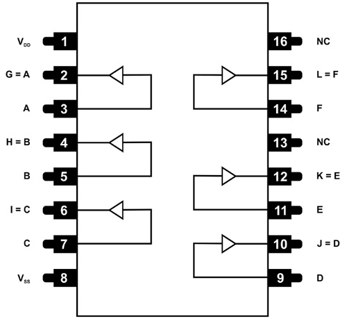
A non-inverting buffer has only one input and only one output and the output is equal to the input. They can be used to produce and increase the propagation delay in a circuit. The image above shows the pin configuration of the IC.
CD4050 IC Internal Schematic and Truth Table
The image below shows how the non-inverting buffers are present in the IC and to which pins. As mentioned earlier, the output is always equal to the input; therefore, input to A(pin 3) will be equal to the output at G (pin 2). Similarly, the outputs will be H=B, I=C, J=D, K=E, L=f.
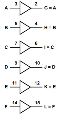
The table below is the truth table of the CD4050 Hex buffer IC. The input and the output of the non-inverter IC are equal.
| Input Signal (A,B,C,D,E,F) | Output Signal(G,H,I,J,K,L) |
| HIGH | HIGH |
| LOW | LOW |
Available Packages
SOIC, PDIP, CDIP
Applications
Here are some of the applications of the Non-Inverter IC.
- HIGH to LOW logic level converter
- DTL or TTL Hex Converters
- As CMOS current sink or source driver


Reviews
There are no reviews yet.